Organic electroluminescent device with hole transmitting regulating and controlling character

An electroluminescent device and hole transport technology, which is applied in the direction of electroluminescent light source, electric solid-state device, electric light source, etc., can solve the problems of high equipment and environment requirements, high device cost, time-consuming and other problems, and achieve good Carrier transport ability, excellent film-forming properties, and the effect of reducing production cost

Inactive Publication Date: 2007-08-22
UNIV OF ELECTRONICS SCI & TECH OF CHINA
View PDF0 Cites 5 Cited by
  • Summary
  • Abstract
  • Description
  • Claims
  • Application Information

AI Technical Summary

Problems solved by technology

[0007] At present, the realization of the organic small molecule hole transport layer that makes up the device usually adopts the method of high vacuum coating, the process is relatively complicated, the requirements for equipment and the environment are high, the energy consumption is high and time-consuming, and the corresponding device cost is relatively high. high

Method used


Image

  • Organic electroluminescent device with hole transmitting regulating and controlling character
  • Organic electroluminescent device with hole transmitting regulating and controlling character
  • Organic electroluminescent device with hole transmitting regulating and controlling character

Examples


Embodiment 1

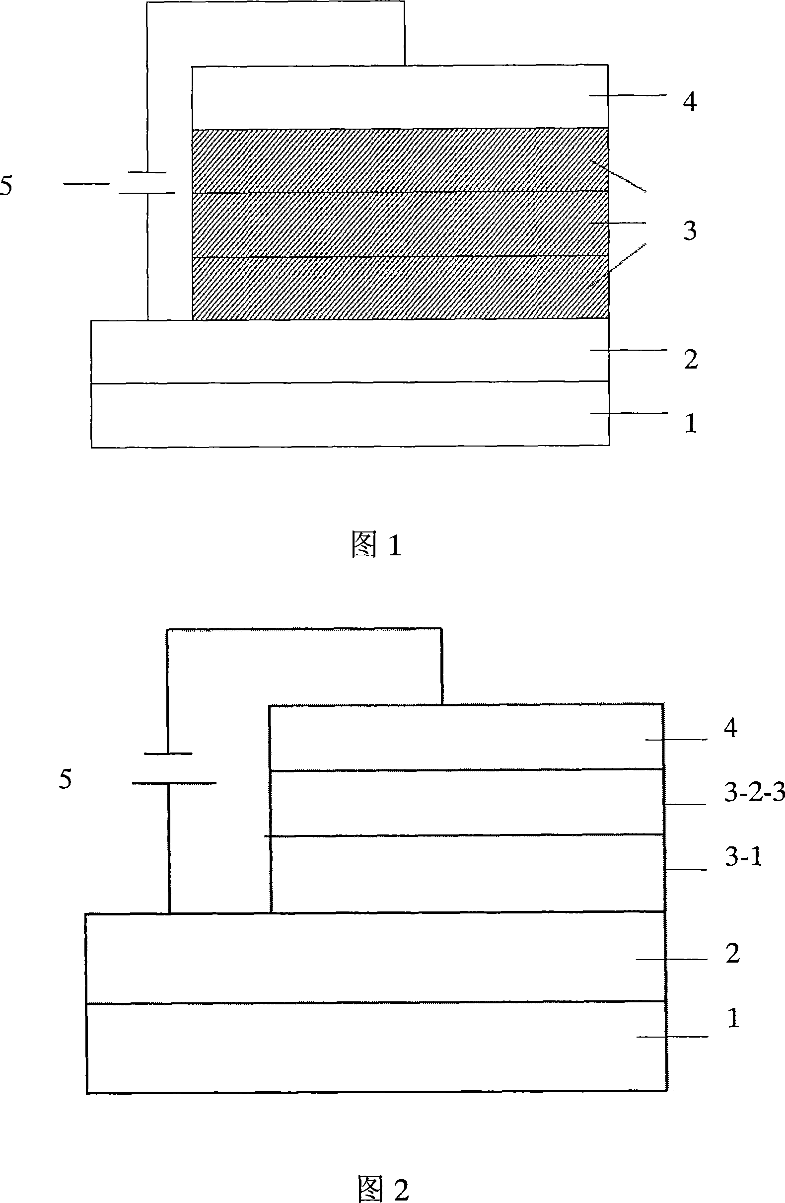
[0049] As shown in FIG. 2, the organic functional layer 3 in the device structure includes a hole transport layer 3-1, a light emitting layer and an electron transport layer 3-2-3.

[0050] The material of the hole transport layer of the device is PS:NPB, and the material of the light emitting layer and electron transport material is Alq 3 , The cathode layer is made of Mg:Ag alloy. The entire device structure is described as:

[0051] Glass substrate / ITO / PS:NPB(100nm) / Alq 3 (50nm) / Mg:Ag(200nm)

[0052] The preparation method is as follows:

[0053] ①Use detergent, ethanol solution and deionized water to ultrasonically clean the transparent conductive substrate ITO glass, and dry it with dry nitrogen after cleaning. Wherein the ITO film on the glass substrate is used as the anode layer of the device, the square resistance of the ITO film is 10O / , and the film thickness is 180nm.

[0054] ② Move the dried substrate into a vacuum chamber, and pretreat the ITO glass with low...

Embodiment 2

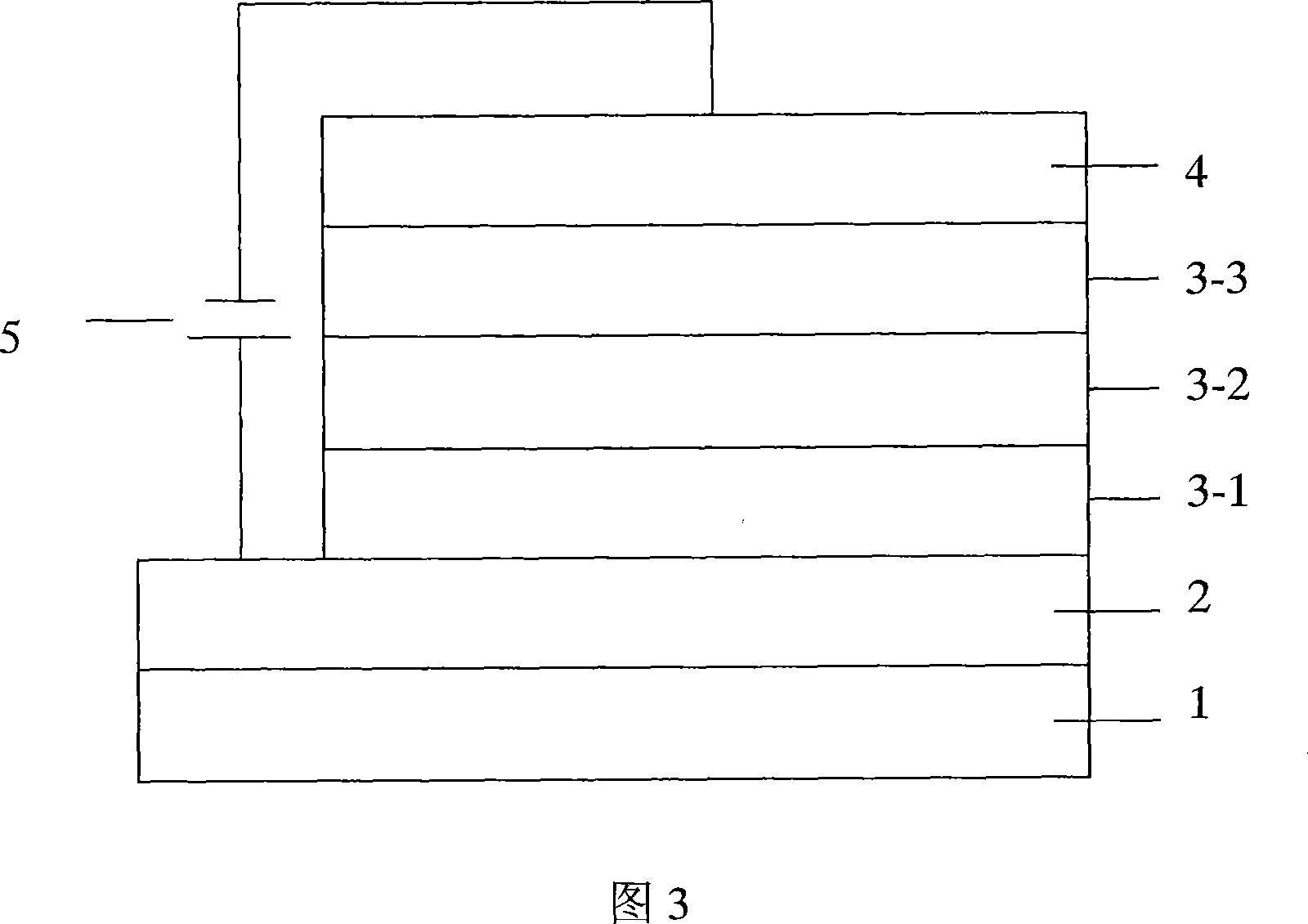
[0061] As shown in FIG. 2, the organic functional layer 3 in the structure of the device includes a hole transport layer 3-1, a light emitting layer and an electron transport layer 3-2-3.

[0062] The material of the hole transport layer of the device is PS:TPD, and the material of the light emitting layer and the electron transport layer is Alq 3 , The cathode layer is made of Mg:Ag alloy. The entire device structure is described as:

[0063] Glass substrate / ITO / PS:TPD(100nm) / Alq 3 The preparation process of the (50nm) / Mg:Ag(100nm) device is similar to that of Example 1.

Embodiment 3

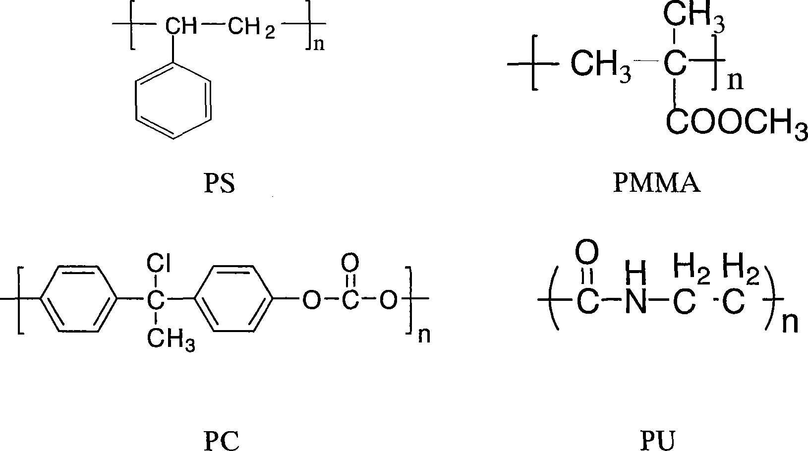
[0065] As shown in FIG. 3 , the organic functional layer 3 in the structure of the device includes a hole transport layer 3 - 1 , a light emitting layer 3 - 2 , and an electron transport layer 3 - 3 .

[0066] The hole transport layer material of the device is PC:TPD, the light emitting layer material is ruberene, and the electron transport material is Bepp 2 , The cathode layer is made of Mg:Ag alloy. The entire device structure is described as:

[0067] Glass substrate / ITO / PC:TPD(100nm) / ruberene(50nm) / Bepp 2 (15nm) / Mg:Ag(100nm)

[0068] The fabrication process of the device is similar to that of Example 1.


PUM


Abstract

This invention discloses an organic electroluminescent device with a cavity transmission adjusting performance including a solid substrate, an anode layer and a cathode layer, in which, an electrode layer is placed on the surface of the solid substrate, an organic functional layer is set between the anode and the cathode layers including a cavity transmission layer and a light emission layer capable of emitting driven by extra fields characterizing that: said cavity transmission layer is the doped system of dielectric polymer material and small molecule cavity transmission material, said organic functional layer also includes an electronic transmission layer, a current carrier injection layer and a buffer layer, in which, the doepd system can adjust and control the cavity transmission performance of small molecules by adjusting the dopent ratio of the basic substance of the polymer and imputies of small molecules.

Description

technical field [0001] The invention relates to the technical field of organic electroluminescence in electronic components, in particular to an organic electroluminescence device with hole transport regulation properties. Background technique [0002] With the continuous improvement of the informatization level of human society, people have higher and higher performance requirements for the carrier of the human-machine interface - the information display device. The continuous progress of display technology and the continuous emergence of new technologies have driven the leapfrog development of the display industry. After undergoing innovations from black and white, color, ultra-flat, flat-screen, and cathode ray tube displays to today's brilliant LCD (liquid crystal display) and PDP (plasma display) flat-panel displays, its industrial scale is getting bigger and bigger. The field of application is also becoming wider and wider. In the field of display, organic electrolum...

Claims


Application Information

Patent Timeline
Patent Type & Authority Applications(China)
IPC IPC(8): H01L51/50H01L51/54H05B33/12
Inventor 于军胜蒋亚东锁钒
Owner UNIV OF ELECTRONICS SCI & TECH OF CHINA
Why Eureka
Try Eureka