
Manufacturing design method for integrated circuit

A manufacturable, initial design technology, used in circuits, semiconductor/solid-state device manufacturing, computing, etc., can solve the problem of not providing unfilled pattern target pattern density, reducing pattern density, etc., to reduce feature size unevenness and grinding. The effect of reducing defects, reducing production costs, and shortening trial production time

Active Publication Date: 2009-12-30
SEMICON MFG INT (SHANGHAI) CORP +1
View PDF5 Cites 0 Cited by
  • Summary
  • Abstract
  • Description
  • Claims
  • Application Information

AI Technical Summary

Problems solved by technology

[0006] The Chinese patent application with the patent number "00806056.8" provides a gate filling method for reducing the pattern density. This method obtains the target pattern density by changing the size of the filling pattern, but does not provide how to obtain the target pattern density when there is no filling pattern , therefore, there is an urgent need for a design method for manufacturability of integrated circuits that can directly obtain the target pattern density by using the existing pattern density

Method used


Image

  • Manufacturing design method for integrated circuit
  • Manufacturing design method for integrated circuit
  • Manufacturing design method for integrated circuit

Examples


Embodiment Construction

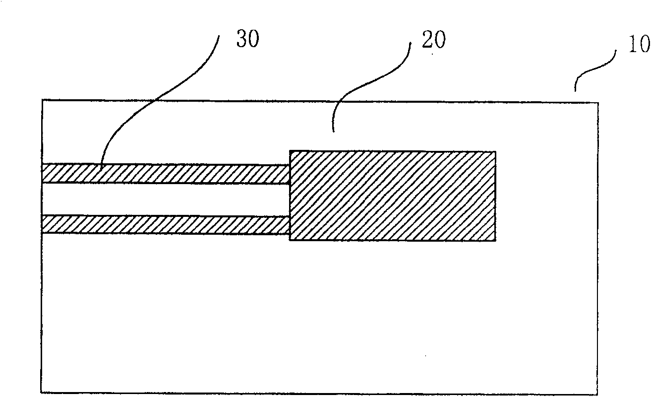
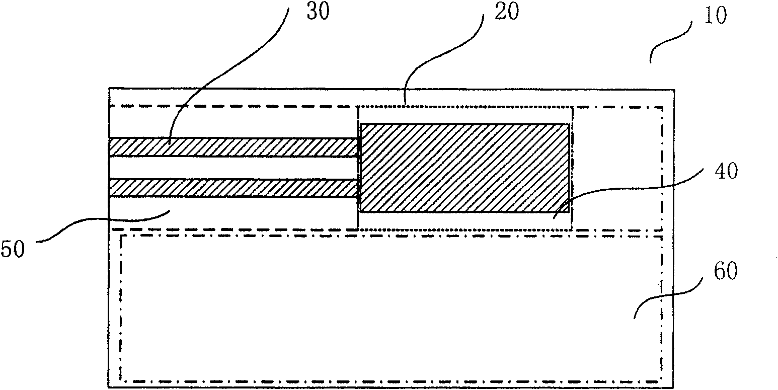
[0069] In order to make the above objects, features and advantages of the present invention more comprehensible, specific implementations of the present invention will be described in detail below in conjunction with the accompanying drawings.

[0070] The method of the present invention is applicable to the design of any layer in the integrated circuit manufacturing process, including: gate layer, diffusion layer and metal layer, etc. In order to avoid unnecessary incomprehension, well-known circuits, systems and process operations are not described.

[0071] The specific process of adopting the method of the present invention is as follows: firstly, density calculation is performed on the initial design graphics, and the density includes local density and overall density; then, the graphic density is extracted, and then the graphic density is adjusted to the target graphic density, and the target graphic density includes The local target pattern density and the overall target...


PUM


Abstract

A manufacturability design method for integrated circuit comprises: a density calculation is carried out on the initial design graph and the density comprises partial density and overall density; the graph density is extracted; the graph density is adjusted until the target graph density is met and the target graph density comprises partial target graph density and overall target graph density; the manufacturability graph density maxim is fixed according to the target graph density; the initial design is improved according to the manufacturability graph density maxim.

Description

technical field [0001] The invention relates to the technical field of semiconductor manufacturing, in particular to a manufacturability design method for integrated circuits. Background technique [0002] The continuous shrinking of integrated circuit (IC) process technology, especially after the 0.13 micron process, the line width of the silicon process is already smaller than the length of the exposure wavelength, making it increasingly difficult to control the stability of the process. It has not been fully considered at the time, that is, the resolution of the process is not enough to accurately convert the geometry designed by the IC engineer to the wafer, making the previous simple design work unacceptable. In this way, it is necessary to repeatedly synthesize and The work of layout and routing, which of course will delay the completion time and cause waste in cost. [0003] The "Design For Manufacturability (DFM)" (Design For Manufacturability, DFM), which aims at t...

Claims


Application Information

Patent Timeline
Patent Type & Authority Patents(China)
IPC IPC(8): H01L21/82H01L27/02G06F17/50
Inventor 许丹傅俊
Owner SEMICON MFG INT (SHANGHAI) CORP
Learn More