
Method for testing GaN single-crystal fault kind and density

A technology of defect types and detection methods, which is applied in the direction of measuring devices, semiconductor/solid-state device testing/measurement, and material analysis through optical means, which can solve the requirements of electrical conductivity, unfavorable averaging of a large number of observations, and the inability to determine the depth of corrosion pits and other issues to achieve the effect of wide applicability

Inactive Publication Date: 2009-01-14
XIDIAN UNIV
View PDF2 Cites 0 Cited by
  • Summary
  • Abstract
  • Description
  • Claims
  • Application Information

AI Technical Summary

Problems solved by technology

They are all effective technical means to characterize the microscopic morphology of the material surface, but each has its own advantages and disadvantages in correctly counting the corrosion pit density: AFM does not require the conductivity of the sample, and can perform depth profile analysis, but the selection and scanning time are longer, It is not conducive to averaging a large number of observations, and is limited by the needle tip effect, and the shape of some corrosion pit surfaces is distorted
SEM is easy to operate and has high precision, but it has requirements for conductivity and cannot determine the depth of corrosion pits
In addition, the existing reports failed to make full use of the advantages of these two techniques to accurately and easily observe the corrosion pit density by optimizing the corrosion conditions.

Method used


Image

  • Method for testing GaN single-crystal fault kind and density
  • Method for testing GaN single-crystal fault kind and density
  • Method for testing GaN single-crystal fault kind and density

Examples


Embodiment Construction

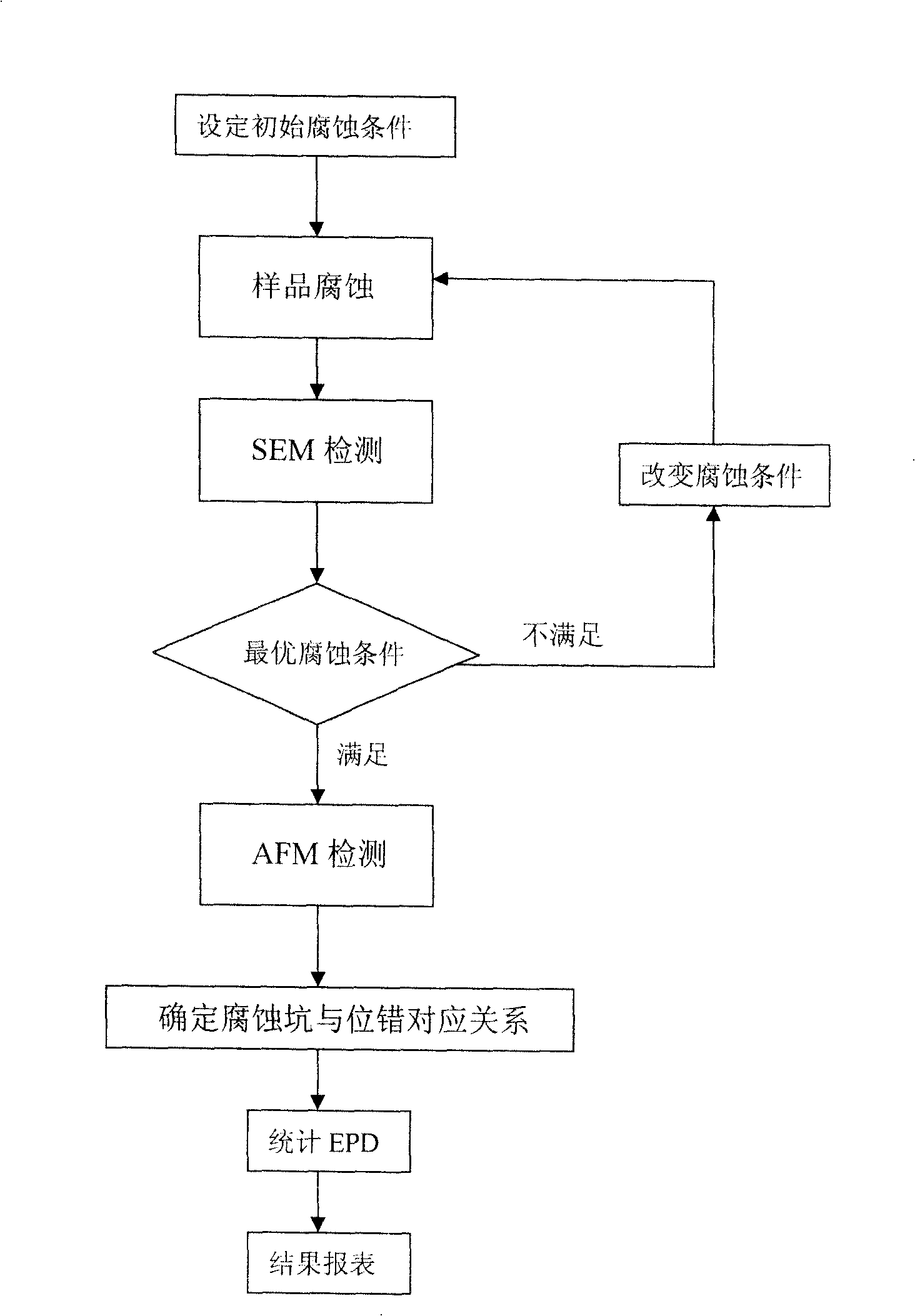
[0033] refer to figure 1 , which is a block flow diagram of the detection method of the present invention, from which the specific steps of the method can be clearly seen. Now combine specific steps and specific examples to illustrate its working process:

[0034] 1. Set the initial corrosion conditions. The initial corrosion temperature and time were estimated from the surface topography of the uncorroded sample.

[0035] 2. Sample corrosion. Clean and remove the organic contamination on the surface of the GaN sample, preheat the crucible to remove the water in it, add KOH particles to heat to the set temperature, put the sample and time it, take out the sample and clean it after the set time. The residual potassium hydroxide is discharged after treatment, and the crucible is cleaned for the next use.

[0036] 3. Carry out SEM detection. On the corroded sample, select nine positions on a wafer or semi-circle, and select more than 3 microscopic areas near each position to...


PUM


Abstract

The invention discloses a detection method of the GaN single-crystal defective kinds and the density which is to improve the traditional wet corrosion detection technology to match the GaN material. The invention detects the surface of the sample by amplifying the SEM magnification times and reducing the AFM detection section step by step. Also it uses the AFM deep section topography and skips over the corrosion condition. It ensures the solid shape of the corrosion pit by compounding the SEM and the AFM to determine the corresponding relation of the corrosion pit and the flaw type by compounding the physical model of the corrosion mechanism. It computes the density and the distributing of all kinds of the flaws by reading the SEM picture. The invention is simple and proper for detecting the industry production.

Description

technical field [0001] The invention relates to the technical field of semiconductor material quality detection, in particular to a detection method for the type and density of GaN single crystal defects, which can be used to determine the type of line defects within 100nm below the surface of a c-plane GaN single crystal thin film grown by heterogeneous epitaxy vs density, suitable for etch pit density EPD at 10 7 ~10 8 / cm 2 Various doped or undoped GaN single crystal materials with good conductivity. Background technique [0002] At present, the most convenient and effective method for the quality inspection of semiconductor single wafers is wet etching, which has been widely used in Si and GaAs materials. There are three keys to this technology: 1. Find the corresponding relationship between corrosion pits and defects to determine the type of defects; 2. Find the optimal corrosion conditions to reveal as many defects as possible; 3. Perform microscopic observation acc...

Claims


Application Information

Patent Timeline
Patent Type & Authority Patents(China)
IPC IPC(8): G01N21/956H01L21/66
Inventor 高志远郝跃张进城李培咸
Owner XIDIAN UNIV
Learn More