Panel display having integrated back grid structure and its manufacturing technology

A flat panel display and back grid technology, which is applied in the manufacture of discharge tubes/lamps, image/graphic display tubes, and cold cathode manufacturing, etc., can solve the problem of relatively high device material requirements, carbon nanotube cathode pollution, and high gate control voltage. problems, to achieve the effect of improving luminous efficiency, improving field emission efficiency, and simplifying the production process

Inactive Publication Date: 2008-12-24
ZHONGYUAN ENGINEERING COLLEGE
View PDF1 Cites 0 Cited by
  • Summary
  • Abstract
  • Description
  • Claims
  • Application Information

AI Technical Summary

Problems solved by technology

At present, in most flat panel display devices, the gate structure is located above the carbon nanotube cathode. The strong control effect of the gate structure is obvious, but the formed gate current is relatively large, and the gate control voltage is relatively high. , the requirements for the material of the device are relatively high, and the carbon nanotube cathode is easy to be polluted and damaged during the manufacturing process of the device, which is its disadvantage

Method used


Image

  • Panel display having integrated back grid structure and its manufacturing technology
  • Panel display having integrated back grid structure and its manufacturing technology
  • Panel display having integrated back grid structure and its manufacturing technology

Examples


Embodiment Construction

[0041] The present invention will be further described below in conjunction with the accompanying drawings and embodiments, but the present invention is not limited to these embodiments.

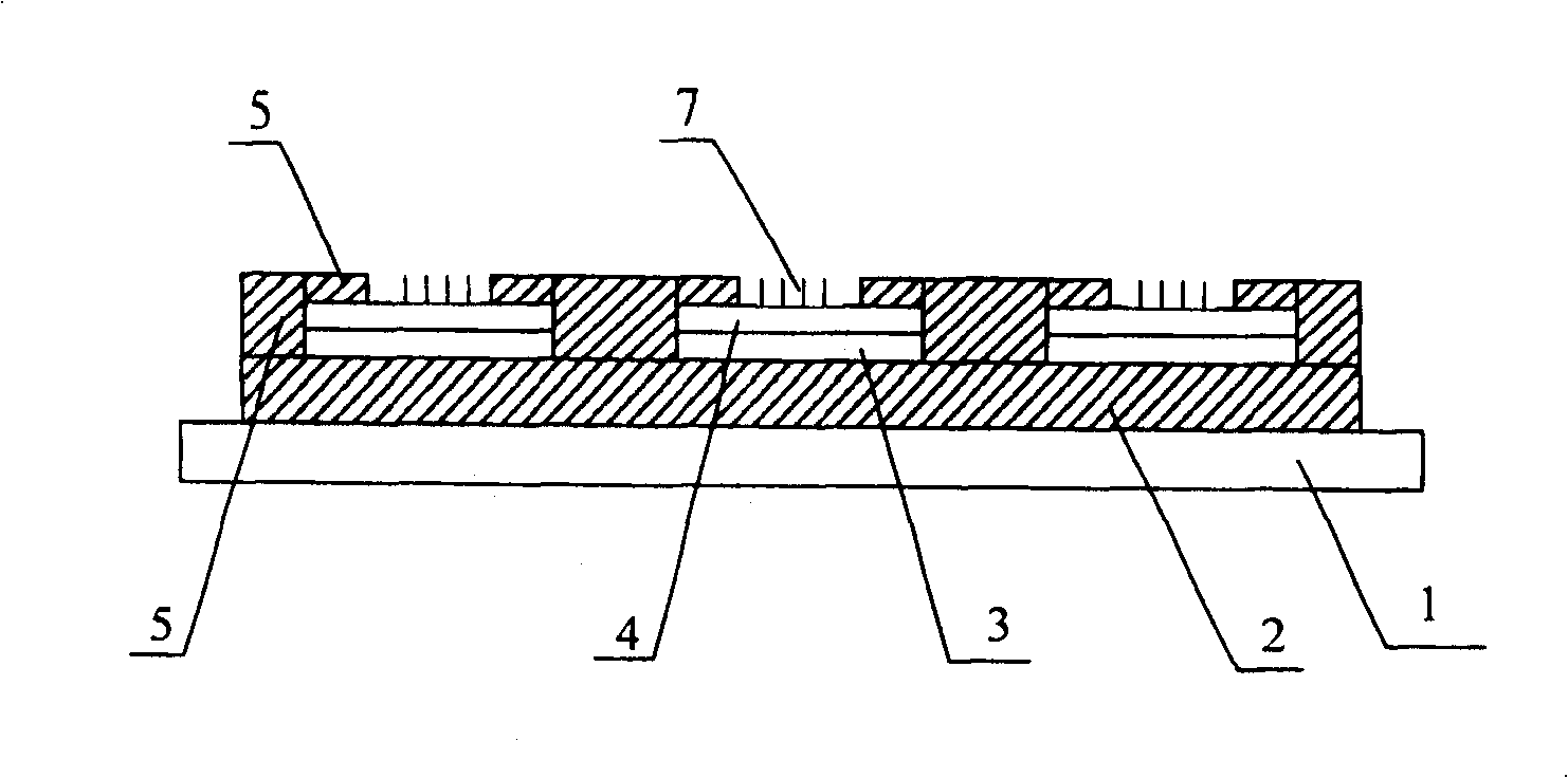
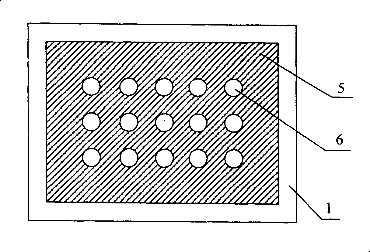
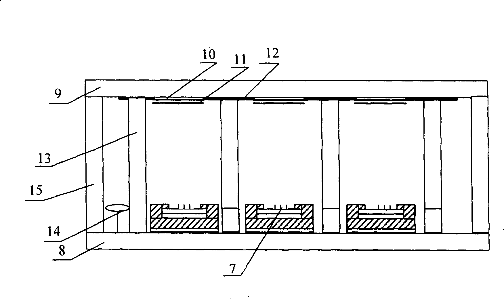
[0042] The present invention comprises a sealed vacuum chamber composed of a cathode panel 8, an anode panel 9 and surrounding glass frames 15; an anode conductive strip 10 and a phosphor layer 11 prepared on the anode conductive strip 10 are arranged on the anode panel 9; The support wall structure 13 between the cathode panel 8 and the anode panel 9 and the getter accessory element 14 are fabricated on the cathode panel 8 with an integrated back grid structure containing the carbon nanotube cathode 7 and controlling the electron emission of the carbon nanotube cathode. The integrated back gate structure includes the base material silicon wafer 1, the first silicon dioxide layer 2 fabricated on the base material silicon wafer 1, and each metal transition formed by photolithography on the fir...


PUM


Abstract

This invention relates to a panel display with an integrated back grating structure and its process method including a sealed vacuum cavity composed of a cathode panel, an anode panel and surrounding glasses, anode conduction strips set on the anode panel and a fluorescence powder layer prepared on the conduction strips, a supporting wall structure between the two panels and getters and an integrated back grating structure prepared on the cathode panel containing carbon nm tube cathode and controlling its electronic emission.

Description

technical field [0001] The invention belongs to the fields of plane display technology, microelectronic science and technology, vacuum science and technology, and nano science and technology, and relates to the manufacture of flat panel field emission displays, in particular to flat panels for carbon nanotube cathodes. The content of device fabrication of field emission display, especially related to the fabrication process of field emission flat panel display device with integrated back gate structure and carbon nanotube cathode. Background technique [0002] Carbon nanotubes have small tip curvature radius, high aspect ratio, extremely high mechanical strength and good physical and chemical properties, and are an ideal cold cathode material. At present, the preparation methods for carbon nanotube cathodes can be roughly divided into two types, namely: direct growth method and transplantation method. The field emission characteristics of carbon nanotube cathodes prepared b...

Claims


Application Information

Patent Timeline
Patent Type & Authority Patents(China)
IPC IPC(8): H01J29/02H01J31/12H01J9/00H01J9/02
Inventor 李玉魁
Owner ZHONGYUAN ENGINEERING COLLEGE
Why Eureka
Try Eureka