Field emission display with plane grid structure and manufacturing technology thereof

A field emission and display technology, used in the manufacture of discharge tubes/lamps, image/graphic display tubes, control electrodes, etc., can solve the problems of large gate current, inability to manufacture large areas, and high requirements for device materials

Inactive Publication Date: 2008-12-24
ZHONGYUAN ENGINEERING COLLEGE
View PDF5 Cites 0 Cited by
  • Summary
  • Abstract
  • Description
  • Claims
  • Application Information

AI Technical Summary

Problems solved by technology

However, the formed gate current is relatively large, and the requirements for the material of the device are relatively high. During the manufacturing process of the device, the carbon nanotube cathode is easily damaged and polluted to a certain extent. This is its disadvantage.
Although the control gate manufacturing materials used by various manufacturing companies or research institutions are different, most of them use special special manufacturing materials and special manufacturing processes, which brings a series of problems, such as : The device manufacturing cost is high; the manufacturing process is complicated; the manufacturing process conditions are too harsh, and large-area manufacturing cannot be carried out, etc.

Method used


Image

  • Field emission display with plane grid structure and manufacturing technology thereof
  • Field emission display with plane grid structure and manufacturing technology thereof
  • Field emission display with plane grid structure and manufacturing technology thereof

Examples


Embodiment Construction

[0042]The present invention will be further described below with reference to the drawings and embodiments, but the present invention is not limited to these embodiments.

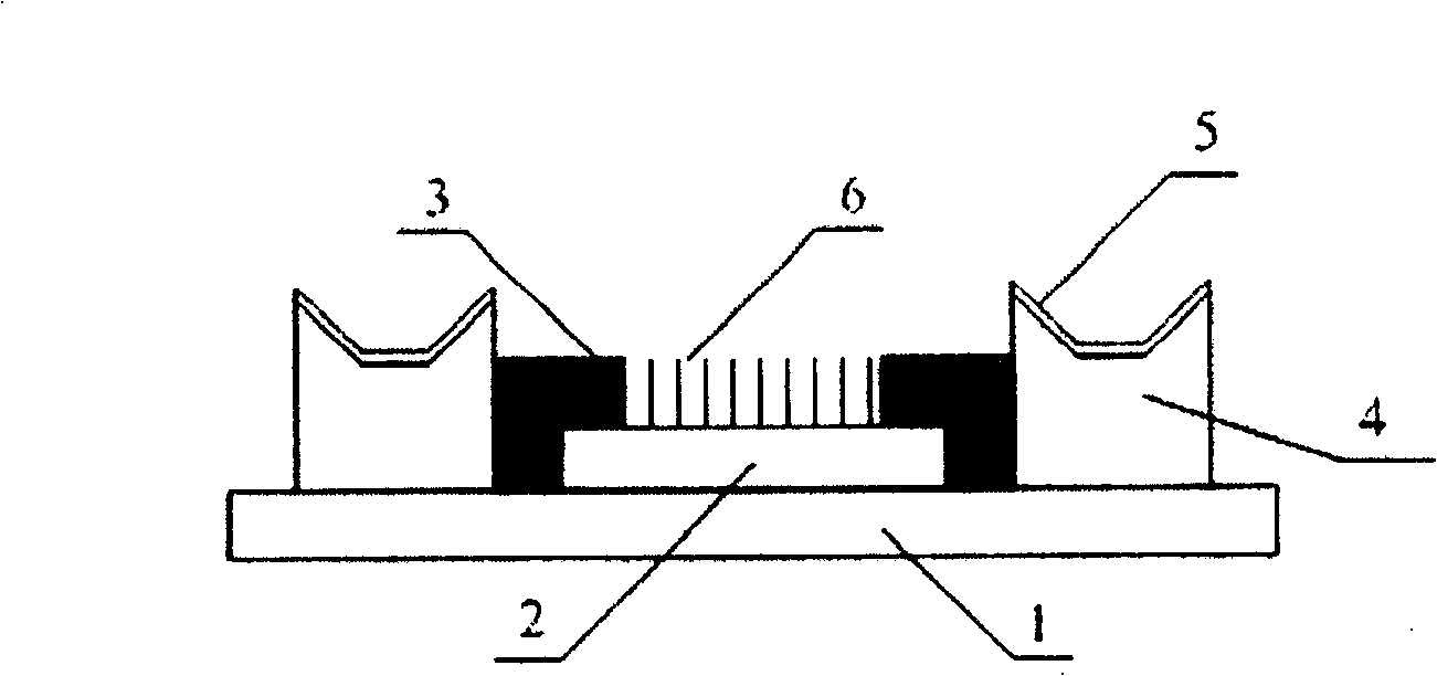
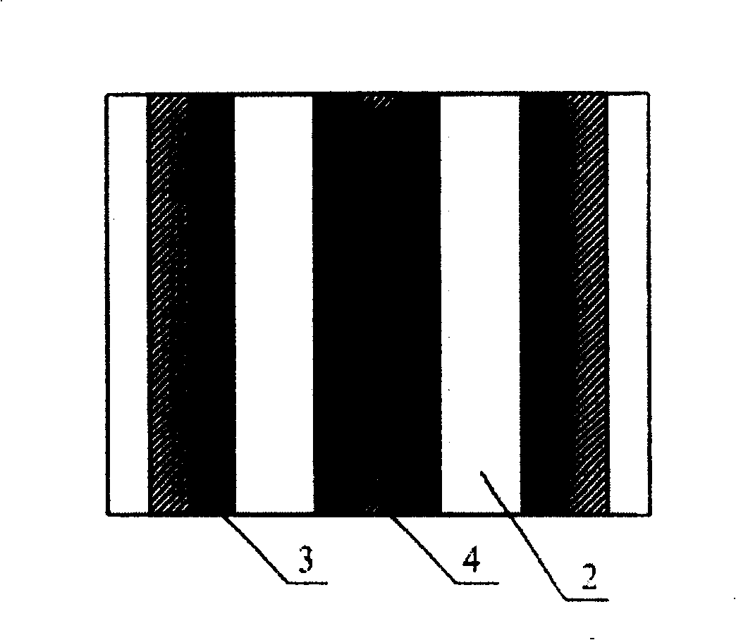
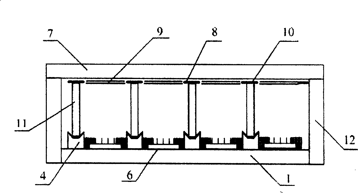
[0043] Such as figure 1 , 2 3, the present invention includes a sealed vacuum chamber composed of an anode panel 7, a cathode panel 1, and a surrounding glass frame 12, a tin indium oxide film layer 8 photoetched on the anode plate 7 and a tin indium oxide film layer 8 prepared on the anode panel 7 The phosphor layer 10 above the thin film layer, the carbon nanotube cathode conductive strip 2 provided on the cathode panel 1, the carbon nanotube cathode 6, the carbon nanotube cathode 6 provided on the carbon nanotube cathode conductive strip 2, and the supporting insulation inside the vacuum chamber The isolation support wall 11 is provided with a flat grid structure for controlling the electron emission of the carbon nanotube cathode 6 on both sides of the carbon nanotube cathode 6 and below the insulating iso...


PUM


Abstract

The invention relates to a field emission display with a flat grid structure and its manufacturing process, comprising a vacuum cavity formed by an anode panel, a cathode panel and surrounding glass frames, a tin-indium oxide thin film layer, and a tin-indium oxide thin-film layer. The phosphor layer, the carbon nanotube cathode conductive strip on the cathode panel, the carbon nanotube cathode on the carbon nanotube cathode conductive strip, the insulating isolation support wall inside the vacuum chamber, and the insulating isolation support wall on both sides of the carbon nanotube cathode A flat grid structure for controlling the electron emission of the carbon nanotube cathode is arranged below, which has the advantages of simple structure, simple manufacturing process, low manufacturing cost, and stable and reliable manufacturing process.

Description

Technical field [0001] The invention belongs to the inter-crossing technical fields of nano science and technology, vacuum microelectronics science and technology, and flat display technology, and relates to the device production of flat-panel field emission displays, and in particular to the triode structure flat-panel field emission displays with carbon nanotube cathodes. The content of the device manufacturing aspect particularly relates to a field emission flat-panel display with a flat grid structure, a carbon nanotube cathode, and a triode structure and the manufacturing process thereof. Background technique [0002] Carbon nanotubes are a special cold cathode material with a high aspect ratio, a small tip curvature radius, and the ability to emit a large number of electrons under the action of an applied voltage, which has attracted people's attention. For flat panel display devices using carbon nanotubes as cathode materials, in order to minimize the production cost and r...

Claims


Application Information

Patent Timeline
Patent Type & Authority Patents(China)
IPC IPC(8): H01J31/12H01J29/02H01J29/46H01J1/46H01J9/02H01J9/00
Inventor 李玉魁
Owner ZHONGYUAN ENGINEERING COLLEGE
Why Eureka
Try Eureka