Differential piesoelectric two dimension acceleration sensor
An acceleration sensor, differential technology, applied in the field of two-dimensional piezoelectric acceleration sensor, can solve the problems of low sensitivity, inability to overcome measurement error, weak output signal, etc., and achieve high sensitivity, light weight, and strong output signal Effect
- Summary
- Abstract
- Description
- Claims
- Application Information
AI Technical Summary
Problems solved by technology
Method used
Image
Examples
Embodiment 1
[0022] Embodiment 1 (with reference to image 3 , 4 , 9, 10):
[0023] This example is an example of improving the reliability of the invention on the basis of the general introduction. Both sides of the four quartz wafers (31, 32, 33, 34) in this example have a relatively long and a relatively short electrode (82, 81) all located in the middle of their upper parts. On the top of the inertial mass 1, there is a cross-shaped wiring groove 11 whose opening corresponds to the electrodes (82, 81) of each quartz wafer (31, 32, 33, 34), and one end is connected to the signal of each electrode (82, 81). After the lead wires 61 gather at the intersection of the cross-shaped wiring groove 11 , they are connected with the connecting plug 7 .
Embodiment 2
[0024] Embodiment 2 (with reference to image 3 , 4 , 5, 6, 7, 8):
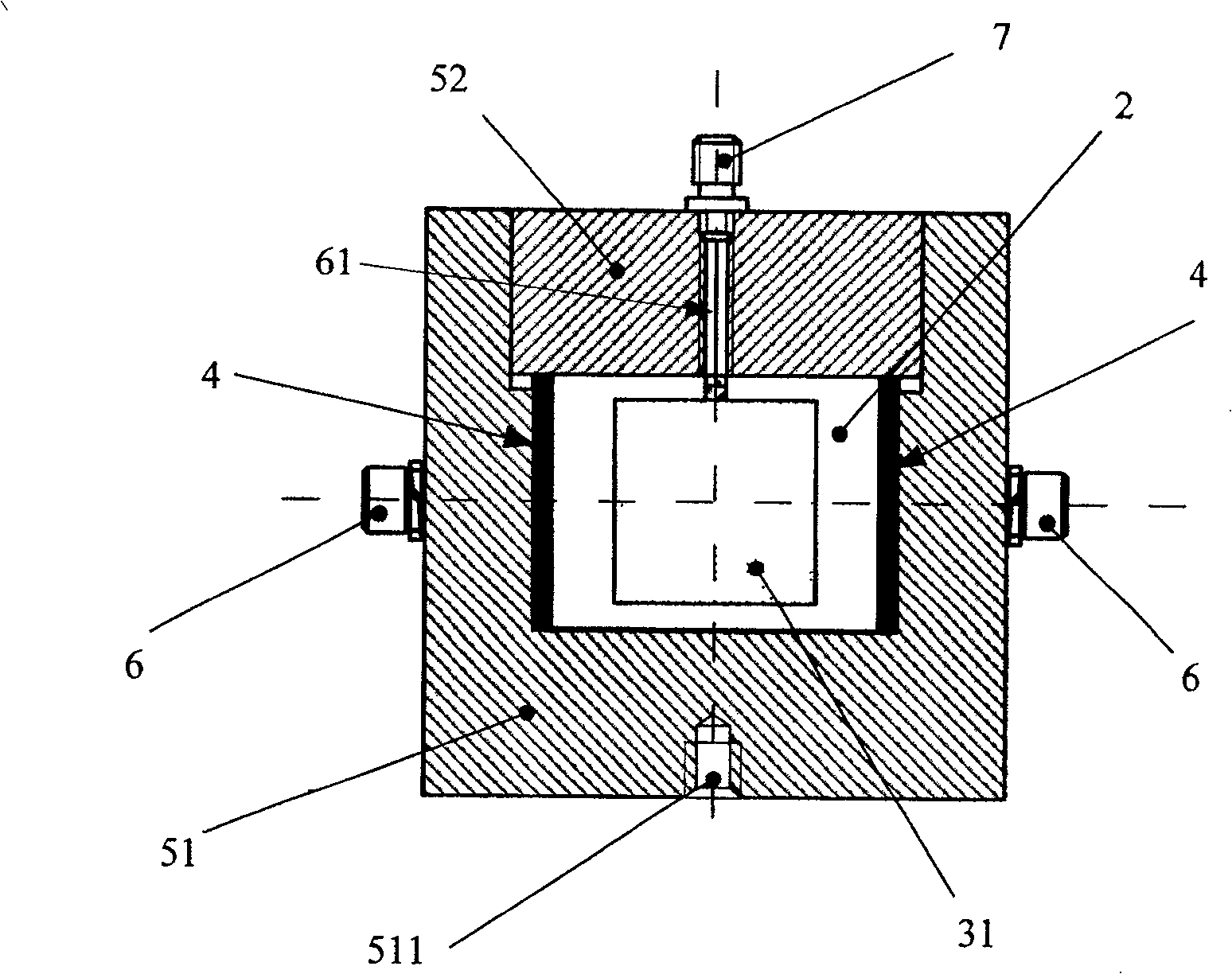
[0025] This example is a good example to further improve the reliability of the invention and ensure the manufacturability on the basis of the general description part or embodiment 1. In this example, the four quartz wafers (31, 32, 33, 34) are all squares whose four sides are parallel to the corresponding surface of the inertial mass 1 but smaller than the corresponding surface. Wherein the power transmission block 4 is equal to the height of the wafer positioning frame 2, equal to the nominal size of the width of the quartz wafer (31, 32, 33, 34) and completely overlapped, but the upper deviation of its width value is not greater than that of the quartz wafer (31, 34). 32,33,34) of the lower deviation---like this, it has been further ensured that the force transmission block 4 can reliably transmit the sensed acceleration signal to the quartz wafer (31,32,33,34).
Embodiment 3
[0026] Embodiment 3 (with reference to image 3 , 4 ):
[0027] This example is an example of further improving the reliability of the invention on the basis of the general introduction, embodiment 1 or embodiment 2. In the base of this example, there is a spacer chamber whose depth is 1-2mm smaller than the height of the wafer spacer 2, and the other corresponding dimensions are equal to the wafer spacer 2, and each of the four walls of the chamber has a depth The positioning groove of the force transmission block 4 that is 0.5 to 1 mm thicker than the force transmission block 4 and whose width is equal to the force transmission block 4 . The case cover 52 of the base is fixed on the case body 51 of its base with its bottom surface and the top surface of the wafer positioning frame 2 with the state of just contacting without applying pressure (that is to say, the case cover 52 is fixedly covered on When on the casing 51 of base, promptly will guarantee the position-limitin...
PUM
 Abstract
Description
Claims
Application Information
 - Generate Ideas
- Intellectual Property
- Life Sciences
- Materials
- Tech Scout
- Unparalleled Data Quality
- Higher Quality Content
- 60% Fewer Hallucinations
Browse by: Latest US Patents, China's latest patents, Technical Efficacy Thesaurus, Application Domain, Technology Topic, Popular Technical Reports.
© 2025 PatSnap. All rights reserved.Legal|Privacy policy|Modern Slavery Act Transparency Statement|Sitemap|About US| Contact US: help@patsnap.com


