Solid camera device, driving method thereof and camera
A technology for solid-state photography and motion, applied in the field of cameras and solid-state photography devices, can solve problems such as long-term and achieve the effect of not sacrificing sensitivity
- Summary
- Abstract
- Description
- Claims
- Application Information
AI Technical Summary
Problems solved by technology
Method used
Image

Examples
Embodiment approach 1
[0140] In Embodiment 1, a CCD (charge-coupled device) sensor of a progressive scanning method will be described as a solid-state imaging device.
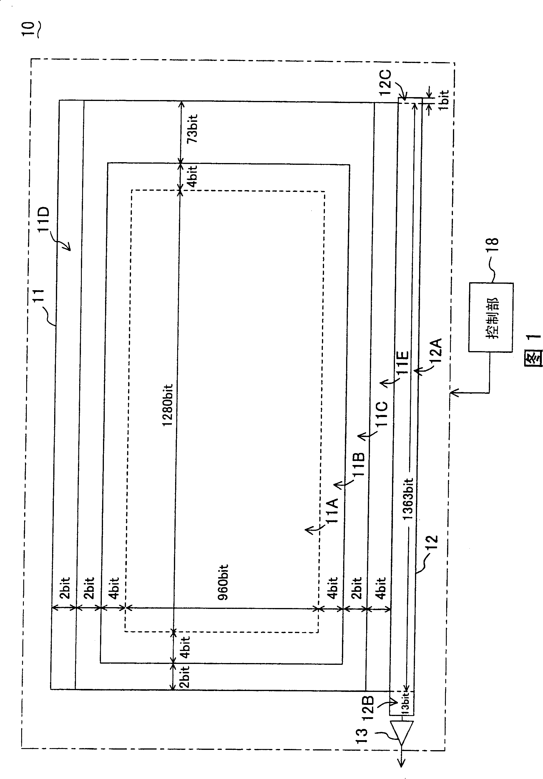
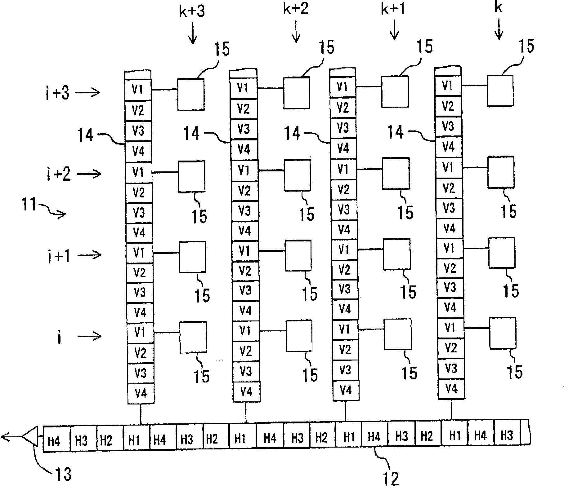
[0141] FIG. 1 is an explanatory diagram showing a configuration example of a CCD sensor 10 according to Embodiment 1 of the present invention. The CCD sensor 10 of FIG. 1 has a pixel section 11 , a horizontal transfer section 12 , a charge detection section 13 , a vertical transfer section (not shown in FIG. 1 ), and a control section 18 . In addition, this CCD sensor 10 employs a simultaneous independent readout method for all pixels.
[0142] The pixel portion 11 has an effective pixel area 11A, a transient area 11B, a shadow area 11C, and vertical empty areas 11D and 11E. The effective pixel area 11A has 1280 (horizontal)×960 (vertical) photodiodes as photoelectric change elements arranged in a matrix. One photodiode constitutes one pixel. Here, the array of pixels in the horizontal direction is called a row, and the array of ...
Embodiment approach 2
[0216] In Embodiment 2, a CCD sensor of an interlaced scanning method will be described as a solid-state imaging device.
[0217] FIG. 17 is an explanatory diagram showing a configuration example of a CCD sensor 30 according to Embodiment 2 of the present invention. The CCD sensor 30 of FIG. 17 has a pixel section 31 , a horizontal transfer section 32 , a charge detection section 33 , a vertical transfer section (not shown in FIG. 17 ), and a control section 38 .
[0218] The pixel section 31 has an effective pixel area 31A, a momentary area 31B, a shadow area 31C, and vertical empty areas 31D and 31E. The effective pixel area 31A has 1280 (horizontal)×960 (vertical) photodiodes as photoelectric conversion elements arranged in a matrix. One photodiode constitutes one pixel. The respective regions 31A to 31E of the pixel unit 31 have the same arrangement as the respective regions 11A to 11E of the pixel unit 11 of the CCD sensor 10 in FIG. 1 , and have the same number of pixe...
Embodiment approach 3
[0258] In Embodiment 3, a MOS (metal oxide semiconductor) sensor, particularly a CMOS (complementary MOS) sensor will be described as a solid-state imaging device.
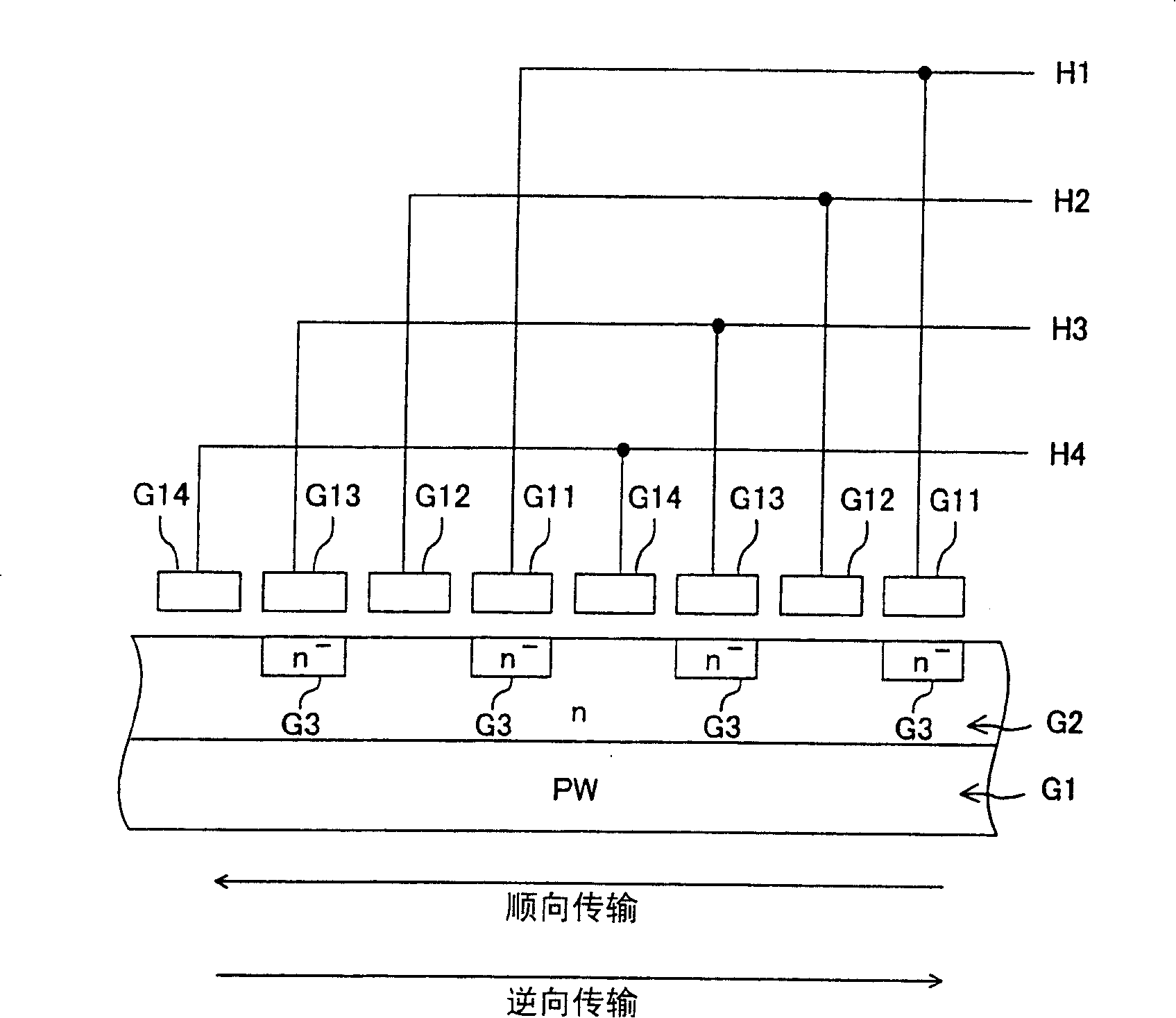
[0259] FIG. 27 is a block diagram showing a configuration example of a CMOS sensor 50 according to Embodiment 3 of the present invention. The CMOS sensor 50 of FIG. 27 has a pixel address specifying circuit 312, a control unit 314, a synchronous signal generator 316, a timing generator 318, a vertical register (row address selection unit) 322, a latch array 324, a horizontal register (column address selection unit) part) 326, a sense amplifier 328 and a pixel part 340.
[0260] The pixel unit 340 has an empty area 342 , an effective pixel area 344 , a light and shadow area 346 , and an empty transfer area 348 . The effective pixel area 344 has 1280 (horizontal)×960 (vertical) photodiodes as photoelectric conversion elements arranged in a matrix. One photodiode constitutes one pixel.
[0261] Figure 28 It is a...
PUM
 Abstract
Description
Claims
Application Information
 - Generate Ideas
- Intellectual Property
- Life Sciences
- Materials
- Tech Scout
- Unparalleled Data Quality
- Higher Quality Content
- 60% Fewer Hallucinations
Browse by: Latest US Patents, China's latest patents, Technical Efficacy Thesaurus, Application Domain, Technology Topic, Popular Technical Reports.
© 2025 PatSnap. All rights reserved.Legal|Privacy policy|Modern Slavery Act Transparency Statement|Sitemap|About US| Contact US: help@patsnap.com