Underlayers And Hardmasks For High-NA EUV: Materials And Etch Selectivity
AUG 22, 20259 MIN READ
Generate Your Research Report Instantly with AI Agent
Patsnap Eureka helps you evaluate technical feasibility & market potential.
High-NA EUV Lithography Background and Objectives
Extreme Ultraviolet (EUV) lithography represents a revolutionary advancement in semiconductor manufacturing, enabling the continuation of Moore's Law by facilitating the production of increasingly smaller transistors. High-NA (Numerical Aperture) EUV lithography, specifically, marks the next evolution in this technology, promising to extend semiconductor scaling beyond the capabilities of standard 0.33 NA EUV systems to 0.55 NA systems.
The development of High-NA EUV technology traces back to the early 2010s when conventional optical lithography reached its physical limits. Standard EUV lithography, operating at 13.5nm wavelength, was commercialized around 2019, but the industry quickly recognized the need for further resolution enhancement to support sub-3nm technology nodes. High-NA EUV emerged as the solution, with ASML announcing its development program in partnership with Zeiss in 2016.
The primary objective of High-NA EUV technology is to achieve approximately 70% improvement in resolution compared to standard EUV systems, enabling feature sizes below 8nm half-pitch. This advancement is critical for the semiconductor industry's roadmap toward 2nm nodes and beyond, supporting increased transistor density and improved device performance while maintaining manufacturing efficiency.
A key technical challenge in High-NA EUV implementation lies in the underlayers and hardmasks that form the foundation of the lithographic process. These materials must demonstrate exceptional etch selectivity to enable precise pattern transfer at extremely small dimensions. The materials must withstand the unique challenges of High-NA EUV exposure, including increased angle of incidence effects and more complex reflection patterns.
The evolution of underlayer and hardmask materials has progressed from traditional carbon-based materials to advanced silicon-containing compounds and metal-based hardmasks. Each generation has aimed to improve etch selectivity, pattern fidelity, and compatibility with increasingly complex multi-patterning schemes required for cutting-edge semiconductor devices.
Current research focuses on developing materials that can provide superior etch selectivity ratios (>10:1) between different layers while maintaining excellent pattern transfer fidelity at dimensions below 10nm. Additionally, these materials must demonstrate compatibility with the anamorphic imaging approach utilized in High-NA EUV systems, which introduces unique challenges in pattern formation and transfer.
The industry trend is moving toward multi-layer stacks with precisely engineered interfaces to optimize both optical properties during exposure and chemical properties during subsequent etch steps. This approach requires interdisciplinary collaboration between material scientists, process engineers, and equipment manufacturers to develop integrated solutions that address the full complexity of High-NA EUV implementation.
Market Demand Analysis for Advanced Semiconductor Nodes
The semiconductor industry's relentless pursuit of Moore's Law has driven demand for advanced lithography technologies, with High-NA EUV (High Numerical Aperture Extreme Ultraviolet) lithography emerging as the critical enabler for nodes below 3nm. Market analysis indicates that the global semiconductor market is projected to reach $1 trillion by 2030, with advanced nodes representing the highest growth segment.
The transition to High-NA EUV technology is primarily driven by the need for increased transistor density in high-performance computing, artificial intelligence processors, and mobile SoCs. TSMC, Samsung, and Intel have all announced massive capital expenditures specifically targeting High-NA EUV implementation, with combined investments exceeding $200 billion over the next five years.
Underlayers and hardmasks represent a crucial but often overlooked segment of this market. The materials science sector supporting these components is experiencing accelerated growth, with specialized chemical suppliers reporting 25-30% annual growth in their advanced lithography materials divisions. The market for High-NA EUV-specific underlayers and hardmasks is expected to grow at a CAGR of 18% through 2028.
Customer requirements are evolving rapidly, with foundries and IDMs demanding materials with unprecedented etch selectivity ratios exceeding 100:1 for certain applications. This represents a significant shift from previous technology nodes where ratios of 30:1 were considered sufficient. The ability to achieve precise pattern transfer at sub-10nm features has become a critical differentiator for material suppliers.
Regional analysis shows Asia-Pacific dominating manufacturing capacity for advanced nodes, with Taiwan maintaining leadership but South Korea and China rapidly expanding capabilities. North America and Europe are focusing on research and development of novel materials, with significant government funding supporting these initiatives through programs like the CHIPS Act and European Chips Act.
The economic impact of delays in High-NA EUV implementation is substantial, with analysts estimating that a six-month delay in node advancement can cost major semiconductor companies billions in lost revenue opportunity. This creates strong financial incentives for accelerated materials development and qualification.
Customer segmentation reveals that while the largest foundries represent the highest volume opportunity, specialized applications in quantum computing and photonics are driving demand for custom underlayer and hardmask solutions with unique properties beyond traditional semiconductor requirements.
Current Underlayer and Hardmask Materials Challenges
The current landscape of underlayer and hardmask materials for High-NA EUV lithography presents significant challenges that require innovative solutions. Traditional materials used in conventional lithography processes are proving inadequate for the extreme requirements of High-NA EUV technology, which demands unprecedented precision at sub-10nm feature sizes.
One of the primary challenges is achieving sufficient etch selectivity between the various layers in the lithographic stack. As pattern dimensions continue to shrink below 10nm, the margin for error in etch processes becomes vanishingly small. Current organic underlayer materials often exhibit insufficient etch selectivity against photoresists, leading to pattern degradation during transfer steps.
Material stability under high-energy EUV exposure represents another critical challenge. The 13.5nm wavelength EUV radiation carries significantly higher photon energy than traditional lithography sources, causing increased chemical modifications and potential degradation of underlayer materials. This can result in line edge roughness and pattern collapse issues that compromise device performance.
Outgassing characteristics of current materials pose serious concerns for High-NA EUV systems. The vacuum environment required for EUV exposure is highly sensitive to contamination, and many conventional underlayer materials release volatile compounds under EUV exposure that can contaminate expensive optics and reduce system uptime.
The thickness control of hardmask materials presents additional difficulties. As pattern aspect ratios increase with smaller feature sizes, hardmasks must be increasingly thin while maintaining sufficient etch resistance. Current silicon-based and metal-based hardmasks often struggle to balance these competing requirements without introducing pattern transfer issues.
Compatibility with complex multi-patterning schemes further complicates material selection. Many existing materials cannot withstand the repeated processing steps required in multi-patterning approaches, leading to cumulative defects and yield loss.
The thermal budget constraints of advanced node processing also limit material options. Many high-performance hardmask materials require high-temperature processing that can damage underlying structures or cause unwanted diffusion in device layers.
Finally, environmental and safety regulations are increasingly restricting the use of certain chemicals traditionally employed in underlayer and hardmask formulations, forcing the industry to develop alternatives with similar performance characteristics but improved sustainability profiles.
Current Underlayer and Hardmask Material Solutions
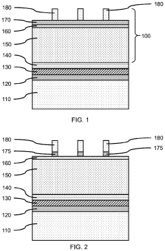
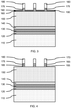
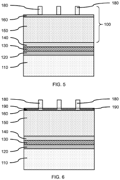
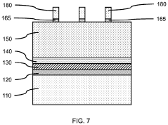
01 Material composition for high etch selectivity hardmasks
Specific material compositions can be used to create hardmasks with high etch selectivity for High-NA EUV lithography. These materials include silicon-rich compounds, metal oxides, and carbon-based materials that provide excellent resistance to etching processes. The composition can be tailored to achieve optimal selectivity ratios between the hardmask and underlying layers, which is crucial for creating high-resolution patterns with minimal feature degradation during the etching process.- Hardmask materials with high etch selectivity for EUV lithography: Various hardmask materials can be used in EUV lithography to achieve high etch selectivity. These materials include silicon-based compounds, metal oxides, and carbon-based materials that provide excellent resistance to etching processes. The hardmask layer protects underlying features during pattern transfer, particularly important in High-NA EUV applications where feature dimensions are extremely small. The high etch selectivity allows for precise pattern transfer with minimal feature degradation.
- Multi-layer underlayer stacks for improved pattern transfer: Multi-layer underlayer stacks can be implemented to enhance pattern transfer in High-NA EUV lithography. These stacks typically consist of different materials with complementary properties, such as an organic planarizing layer combined with a silicon-containing intermediate layer and a top anti-reflective coating. This approach helps manage reflection control while providing the necessary etch selectivity between layers. The multi-layer structure enables more precise pattern transfer and better control of critical dimensions in advanced semiconductor manufacturing.
- Silicon-rich materials for enhanced etch resistance: Silicon-rich materials serve as effective hardmasks and underlayers in High-NA EUV lithography due to their excellent etch resistance properties. Materials such as silicon nitride, silicon carbide, and silicon-rich oxides can be incorporated into the lithographic stack to provide high selectivity during plasma etching processes. These materials form robust protective layers that withstand aggressive etch chemistries while maintaining pattern fidelity, which is crucial for the extremely small feature sizes in High-NA EUV applications.
- Carbon-based hardmask materials for vertical pattern transfer: Carbon-based hardmask materials, including amorphous carbon, diamond-like carbon, and spin-on carbon layers, provide exceptional etch selectivity in High-NA EUV lithography. These materials offer high resistance to oxygen-based and fluorine-based plasma etching processes, enabling highly anisotropic pattern transfer with minimal lateral etching. The carbon-based hardmasks can be deposited in thin, uniform layers and are particularly effective for creating high-aspect-ratio features with vertical sidewalls, which is essential for advanced semiconductor device fabrication.
- Etch process optimization for High-NA EUV pattern transfer: Optimizing etch processes is crucial for achieving high selectivity in High-NA EUV lithography. This includes careful selection of etch gases, plasma conditions, and process parameters tailored to the specific hardmask and underlayer materials used. Advanced techniques such as atomic layer etching, cyclic etch-passivation processes, and multi-step etch sequences can be employed to enhance selectivity and maintain critical dimensions. Process optimization also involves managing etch byproducts and minimizing pattern collapse in high-aspect-ratio features, which becomes increasingly challenging at the dimensions required for High-NA EUV lithography.
02 Multi-layer hardmask structures for improved pattern transfer
Multi-layer hardmask structures can be implemented to enhance pattern transfer in High-NA EUV lithography. These structures typically consist of alternating layers with different etch characteristics, allowing for precise control of the etching process. The combination of different materials in the stack enables the creation of high-aspect-ratio features while maintaining pattern fidelity. This approach is particularly valuable for complex semiconductor device fabrication requiring extremely fine features.Expand Specific Solutions03 Underlayer formulations for enhanced adhesion and etch resistance
Specialized underlayer formulations can be developed to provide both enhanced adhesion to substrates and superior etch resistance. These formulations often incorporate polymeric materials with specific functional groups that improve adhesion to various substrate materials while maintaining compatibility with overlying photoresist layers. The chemical composition can be optimized to withstand aggressive etch chemistries used in High-NA EUV processes, preventing pattern collapse and ensuring dimensional accuracy of transferred features.Expand Specific Solutions04 Etch process optimization for High-NA EUV patterning
Optimizing etch processes specifically for High-NA EUV patterning involves careful selection of etch gases, power settings, and chamber conditions. These optimizations can significantly improve the selectivity between hardmasks, underlayers, and substrate materials. Advanced techniques such as atomic layer etching and cyclic etch-passivation processes can be employed to achieve near-vertical sidewalls and minimal line edge roughness, which are critical for high-resolution High-NA EUV lithography applications.Expand Specific Solutions05 Integration schemes for hardmasks and underlayers in advanced node processes
Integration schemes for hardmasks and underlayers in advanced node processes require careful consideration of material compatibility, thermal budgets, and process sequences. These schemes often involve strategic placement of etch stop layers, careful management of film stress, and minimization of interfacial mixing between layers. Novel approaches include the use of self-assembled materials and hybrid organic-inorganic compositions that can be precisely tuned for specific applications in High-NA EUV lithography, enabling the fabrication of increasingly complex semiconductor devices at sub-10nm nodes.Expand Specific Solutions
Key Industry Players in High-NA EUV Materials Development
The high-NA EUV underlayers and hardmasks market is currently in a growth phase, with the technology approaching early maturity as semiconductor manufacturing advances toward 3nm and below nodes. The market is projected to expand significantly as high-NA EUV lithography becomes essential for next-generation chip production. Leading equipment suppliers Applied Materials, Lam Research, and Tokyo Electron are competing to develop advanced materials with superior etch selectivity properties, while semiconductor manufacturers like Samsung, TSMC, and Intel drive demand through implementation in their advanced nodes. GLOBALFOUNDRIES and Micron are also investing in compatible materials research. The competitive landscape shows material innovation focusing on improved etch resistance, pattern transfer fidelity, and compatibility with increasingly complex multi-patterning schemes required for high-NA EUV implementation.
Applied Materials, Inc.
Technical Solution: Applied Materials has developed advanced underlayer and hardmask solutions specifically engineered for High-NA EUV lithography. Their technology focuses on multi-layer stack approaches that combine spin-on carbon hardmasks with silicon-rich anti-reflective coatings. The company's Endura® platform integrates PVD (Physical Vapor Deposition) and CVD (Chemical Vapor Deposition) processes to create highly uniform hardmask layers with precisely controlled optical properties. Their latest innovation includes metal-based hardmasks with enhanced etch selectivity ratios exceeding 100:1 when compared to conventional photoresists, enabling the creation of high-aspect-ratio features below 10nm. Applied Materials has also developed specialized etch chemistries that maintain critical dimension uniformity while providing the selectivity needed for High-NA EUV processes. Their integrated approach combines materials engineering with process control to address the increased challenges of reflection control and pattern transfer in High-NA EUV lithography.
Strengths: Comprehensive materials portfolio with integrated deposition and etch solutions; proven track record in high-volume manufacturing environments; strong R&D capabilities for next-generation materials. Weaknesses: Higher implementation costs compared to conventional solutions; requires significant process integration work for optimal performance; some solutions may require specialized equipment upgrades.
Lam Research Corp.
Technical Solution: Lam Research has pioneered advanced hardmask and underlayer solutions specifically designed for High-NA EUV lithography challenges. Their Sense.i® etching platform incorporates specialized plasma chemistry optimization for high-selectivity etching of complex multi-layer stacks. Lam's approach focuses on atomic-level precision in material removal, with their proprietary hardmask materials demonstrating etch selectivity ratios of up to 150:1 relative to EUV photoresists. The company has developed novel organosilicon-based underlayers that provide both anti-reflective properties and enhanced pattern transfer capabilities. Their integrated hardmask solution combines titanium-based materials with advanced carbon compositions to enable the extreme aspect ratios required for sub-10nm features. Lam Research's technology also addresses the critical challenge of line edge roughness in High-NA EUV processes through specialized smoothing techniques applied during the pattern transfer process. Their materials are engineered to minimize pattern collapse while maintaining dimensional accuracy throughout the multi-step etch process required for advanced node manufacturing.
Strengths: Industry-leading etch selectivity ratios; comprehensive process integration capabilities; materials specifically optimized for EUV wavelengths. Weaknesses: Higher material costs compared to conventional approaches; requires specialized equipment configurations; more complex process flows that may impact throughput.
Critical Patents and Research in High-NA EUV Materials
Patterning scheme to improve EUV resist and hard mask selectivity
PatentWO2020014179A1
Innovation
- A method involving a film stack with a bottom layer of diamond-like carbon, a middle layer that can be selectively etched relative to a photoresist, and a hard mask structure, where the middle layer is converted to increase etch selectivity, using EUV radiation and plasma processes to achieve high selectivity and minimize linewidth variations.
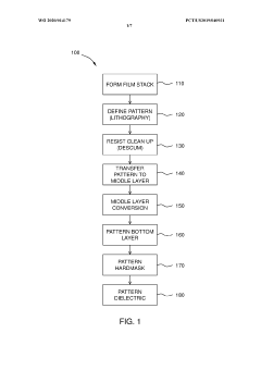
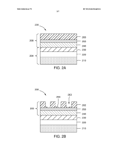
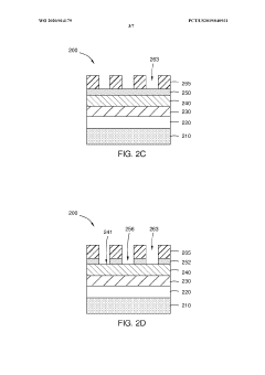
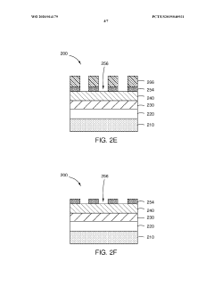
Extreme ultraviolet (EUV) mask stack processing
PatentActiveUS11131919B2
Innovation
- A method involving the formation of resist templates on an upper hardmask layer, followed by a dry etch process to modify and activate the surfaces, allowing for the exposure of an underlying organic planarization layer without photoresist patterning loss, using a gas phase hardmask etch that is highly selective to photoresist material and effective for high aspect ratio features.
Supply Chain Analysis for EUV Materials Ecosystem
The EUV materials ecosystem represents a complex and highly specialized supply chain that is critical to the advancement of high-NA EUV lithography technology. This ecosystem encompasses multiple tiers of suppliers, from raw material producers to specialized chemical manufacturers who develop underlayers and hardmasks with precise etch selectivity properties.
Primary material suppliers for EUV underlayers and hardmasks include global chemical giants such as JSR Corporation, Shin-Etsu Chemical, TOK, and DuPont, who have established dominant positions through decades of expertise in semiconductor materials. These companies maintain sophisticated R&D facilities dedicated to developing next-generation materials that can meet the increasingly stringent requirements of high-NA EUV processes.
The supply chain exhibits significant geographical concentration, with Japan and the United States hosting the majority of advanced material development and production capabilities. This concentration creates potential vulnerabilities in the global semiconductor manufacturing ecosystem, particularly as geopolitical tensions increase and nations prioritize technological sovereignty.
Material qualification processes represent a critical bottleneck in the supply chain. New underlayer and hardmask materials typically require 18-24 months of rigorous testing before integration into production environments. This extended qualification timeline creates significant barriers to entry for new suppliers and compounds supply chain risks when material specifications change rapidly.
Specialized equipment for material characterization and testing forms another crucial segment of the ecosystem. Companies like KLA Corporation and Applied Materials provide the metrology and analytical tools necessary to evaluate etch selectivity and other critical parameters of EUV materials. The availability of these specialized tools can significantly impact material development cycles.
Raw material dependencies create additional supply chain vulnerabilities. Many advanced underlayer and hardmask formulations rely on rare elements or specialized polymers with limited sourcing options. For instance, certain metal-containing hardmasks require specific organometallic compounds that may have only one or two global suppliers.
The ecosystem is further complicated by intellectual property considerations, with most leading suppliers maintaining extensive patent portfolios around their material formulations. This IP landscape creates complex licensing requirements and potential legal barriers that new entrants must navigate to participate in the market.
Recent supply chain disruptions have highlighted the fragility of this ecosystem, with several major semiconductor manufacturers reporting material shortages that directly impacted their high-NA EUV implementation timelines. These disruptions have accelerated industry efforts to develop more resilient supply chains through supplier diversification and localized production capabilities.
Environmental Impact of Advanced Lithography Materials
The environmental impact of advanced lithography materials, particularly those used in High-NA EUV processes including underlayers and hardmasks, presents significant sustainability challenges for the semiconductor industry. These specialized materials, while critical for achieving nanometer-scale features, often contain perfluorinated compounds, metal-organic complexes, and other persistent chemicals that pose environmental concerns throughout their lifecycle.
Manufacturing of underlayers and hardmasks typically involves energy-intensive processes and hazardous precursors. The production of fluorinated polymers commonly used in these applications generates greenhouse gas emissions with global warming potentials thousands of times greater than CO2. Additionally, the synthesis of metal-containing hardmasks often requires rare earth elements and precious metals, contributing to resource depletion and mining-related environmental degradation.
During semiconductor fabrication, the etching processes that rely on the selectivity properties of these materials consume substantial quantities of perfluorinated gases such as CF4, C2F6, and NF3. These gases have atmospheric lifetimes measured in thousands of years and contribute significantly to climate change when released. The plasma etching processes also generate toxic byproducts including fluorinated compounds and volatile metal species that require specialized abatement systems.
Waste management presents another environmental challenge. Chemical mechanical planarization slurries containing nanoparticles, spent developer solutions, and etching residues must undergo extensive treatment before disposal. Many of these materials resist conventional wastewater treatment methods, potentially leading to persistent environmental contamination if not properly managed.
Recent industry initiatives have focused on developing more sustainable alternatives. Bio-based underlayers derived from renewable resources show promise for reducing carbon footprints, while metal hardmasks utilizing more abundant elements like silicon and aluminum aim to decrease reliance on scarce materials. Advanced recycling technologies for recovering precious metals from spent materials are also emerging as important sustainability measures.
Regulatory frameworks worldwide are increasingly addressing these environmental concerns. The European Union's REACH regulations and similar initiatives in Asia and North America are driving manufacturers to phase out particularly harmful substances and develop greener alternatives. Industry consortia like SEMI and IRDS have established roadmaps for environmental sustainability that specifically target lithography material improvements.
As High-NA EUV technology advances toward commercialization, balancing performance requirements with environmental considerations will remain a critical challenge. Future research must focus on developing materials with comparable etch selectivity but reduced environmental impact throughout their lifecycle.
Unlock deeper insights with Patsnap Eureka Quick Research — get a full tech report to explore trends and direct your research. Try now!
Generate Your Research Report Instantly with AI Agent
Supercharge your innovation with Patsnap Eureka AI Agent Platform!