Defectivity Control For Contact And Via Layers With EUV Resists
AUG 22, 20259 MIN READ
Generate Your Research Report Instantly with AI Agent
Patsnap Eureka helps you evaluate technical feasibility & market potential.
EUV Resist Technology Background and Objectives
Extreme Ultraviolet (EUV) lithography represents a revolutionary advancement in semiconductor manufacturing, enabling the continuation of Moore's Law by facilitating the production of increasingly smaller and more densely packed integrated circuits. The evolution of EUV technology began in the late 1990s, with significant research investments from industry consortia and semiconductor giants seeking alternatives to traditional deep ultraviolet (DUV) lithography as feature sizes approached fundamental physical limits.
The development trajectory of EUV lithography has been marked by persistent engineering challenges, particularly in the realm of photoresist technology. Early EUV resist materials exhibited limitations in sensitivity, resolution, and line edge roughness—a trilemma that continues to challenge researchers. The industry has progressed from first-generation chemically amplified resists (CARs) to more sophisticated metal-oxide based formulations designed specifically for the 13.5nm wavelength of EUV light.
The primary technical objective in EUV resist development is to achieve defect-free patterning of contact and via layers at dimensions below 20nm. These critical structures serve as vertical interconnects between different metal layers in integrated circuits, and their integrity directly impacts device performance and yield. Defectivity control has emerged as a paramount concern as the industry transitions from research to high-volume manufacturing with EUV technology.
Current industry targets include achieving defect densities below 0.01 defects/cm² for critical layers, with particular emphasis on eliminating pattern collapse, missing contacts, and bridging defects that disproportionately affect high-aspect-ratio features. The technical roadmap also prioritizes improving resist sensitivity to reduce exposure times while maintaining acceptable line edge roughness (LER) and line width roughness (LWR) metrics.
The global semiconductor industry has coalesced around several key performance indicators for next-generation EUV resists, including resolution capability below 8nm half-pitch, sensitivity thresholds of <20mJ/cm², and LER/LWR values under 2nm. These ambitious targets reflect the increasing demands of advanced logic and memory applications that require precise control of nanoscale features.
Looking forward, the technology evolution trend points toward hybrid resist systems that combine the advantages of traditional organic materials with inorganic components to enhance etch resistance and pattern fidelity. Concurrent development of complementary technologies such as underlayers, topcoats, and post-exposure processing techniques further aims to mitigate defectivity challenges in contact and via formation.
The convergence of material science, chemical engineering, and optical physics continues to drive innovation in this field, with the ultimate goal of enabling semiconductor devices at the 3nm node and beyond while maintaining economically viable manufacturing processes.
Market Demand for Advanced Semiconductor Nodes
The semiconductor industry's relentless pursuit of Moore's Law has driven the transition to advanced nodes below 7nm, creating substantial market demand for EUV lithography solutions, particularly for critical contact and via layers. This demand is primarily fueled by leading-edge logic and memory manufacturers seeking to maintain competitive advantages through higher performance, lower power consumption, and increased transistor density.
Market analysis indicates that the global semiconductor equipment market specifically related to EUV lithography is experiencing robust growth, with the EUV segment expanding at a compound annual growth rate exceeding traditional DUV lithography equipment. This growth trajectory is directly linked to the increasing adoption of EUV technology for critical layers in advanced node manufacturing.
The economic drivers behind this market demand are compelling. While EUV lithography systems represent significant capital investments, they enable process simplification by reducing multi-patterning steps required with traditional lithography. This simplification translates to lower overall production costs and improved yields for complex contact and via layers, which have historically been yield-limiting factors in advanced semiconductor manufacturing.
Leading foundries and memory manufacturers have accelerated their EUV implementation roadmaps, particularly for nodes at 5nm and below, where the economic and technical benefits of EUV for contact and via layers become most pronounced. Market research indicates that approximately 75% of leading-edge logic manufacturing will incorporate EUV lithography for critical layers by 2025.
The geographical distribution of this market demand shows concentration in East Asia, particularly Taiwan, South Korea, and increasingly China, followed by the United States and Europe. This distribution aligns with the locations of major semiconductor manufacturing facilities investing in advanced nodes.
Customer requirements driving this market demand include improved defectivity control specifically for contact and via layers, as these features become increasingly challenging at smaller dimensions. End-user industries—particularly high-performance computing, artificial intelligence accelerators, and mobile processors—are demanding chips with higher transistor densities that can only be economically manufactured using EUV lithography with specialized resists.
The market is further stimulated by national initiatives to strengthen domestic semiconductor manufacturing capabilities, with significant government investments in the United States, Europe, Japan, South Korea, and China all including provisions for advanced lithography capabilities, including EUV technology for critical layers.
EUV Resist Defectivity Challenges
Extreme Ultraviolet (EUV) lithography represents a revolutionary advancement in semiconductor manufacturing, enabling the continuation of Moore's Law through the production of increasingly smaller feature sizes. However, as the industry transitions to EUV technology, resist defectivity has emerged as a critical challenge, particularly for contact and via layers where dimensional precision is paramount.
EUV resists face unique defectivity challenges compared to traditional 193nm immersion lithography resists. The high-energy photons (13.5nm) in EUV lithography generate secondary electrons that can cause unintended chemical reactions in the resist material, leading to pattern distortion and defect formation. These defects manifest as missing contacts, bridging between features, and irregular shapes that compromise device functionality.
Material-related defects in EUV resists often stem from their complex chemical composition. Modern EUV resists typically contain metal oxide nanoparticles to enhance sensitivity, but these can aggregate and create non-uniform distributions within the resist film. Additionally, the interaction between resist components and substrate materials can lead to interface defects that are particularly problematic for contact and via layers where vertical profile control is essential.
Process-induced defects represent another significant challenge. The limited photon flux in current EUV systems necessitates highly sensitive resists, which often exhibit narrow process windows. This sensitivity makes EUV resists particularly vulnerable to variations in exposure dose, post-exposure bake conditions, and development parameters. Even minor fluctuations can result in critical dimension variations and defect formation in contact holes and vias.
Contamination-related defects are exacerbated in EUV lithography due to the vacuum environment required for operation. Organic contaminants from resist outgassing can deposit on optical surfaces, reducing system performance over time. Furthermore, metallic contamination from resist components can migrate during processing, creating electrical shorts or opens in the final device structure.
Pattern collapse represents a particularly severe challenge for high-aspect-ratio features like contacts and vias. As feature sizes decrease and aspect ratios increase, capillary forces during the development and drying processes can cause adjacent features to bend and touch, creating bridging defects. This phenomenon becomes more pronounced with EUV resists due to their typically lower mechanical strength compared to traditional resists.
Line edge roughness (LER) and line width roughness (LWR) are inherent challenges in EUV lithography that directly impact contact and via quality. The stochastic nature of EUV photon absorption and the subsequent chemical amplification process lead to statistical variations in feature edges, which can significantly impact device performance, particularly in critical contact areas where precise dimensions are essential for proper electrical connectivity.
Current Defectivity Control Methods for EUV Lithography
01 Resist material composition optimization
Optimizing the chemical composition of EUV resist materials is crucial for defectivity control. This includes developing specialized polymers, photoacid generators, and additives that minimize pattern collapse and improve resolution. Advanced resist formulations can reduce line edge roughness and pattern bridging while enhancing sensitivity to EUV radiation, thereby decreasing defect rates in the lithography process.- Resist material composition optimization: Optimizing the chemical composition of EUV resist materials is crucial for defectivity control. This includes developing specialized polymers, photoacid generators, and additives that minimize pattern collapse and improve resolution. Advanced resist formulations can reduce line edge roughness and pattern bridging while enhancing sensitivity to EUV radiation, thereby decreasing defect rates in the lithography process.
- Process parameter control and monitoring: Precise control and real-time monitoring of process parameters are essential for minimizing defects in EUV lithography. This includes optimizing exposure dose, post-exposure bake temperature, development time, and other critical parameters. Advanced metrology systems can detect variations in process conditions that might lead to defects, allowing for immediate adjustments to maintain optimal performance and reduce defectivity.
- Contamination control techniques: Controlling contamination is vital for EUV resist defectivity management. This involves implementing advanced filtration systems, clean room protocols, and specialized handling procedures to prevent particle contamination. Techniques such as resist purification, substrate cleaning, and environmental control in the lithography area significantly reduce defects caused by foreign particles and chemical impurities in the resist material.
- Advanced inspection and defect analysis: Implementing sophisticated inspection and analysis techniques enables early detection and characterization of defects in EUV resists. This includes using electron microscopy, optical inspection tools, and machine learning algorithms to identify defect patterns and root causes. Automated defect classification systems help categorize defects by type and origin, facilitating targeted process improvements and defect reduction strategies.
- Pattern design optimization: Optimizing pattern design for EUV lithography can significantly reduce defectivity. This involves implementing design rules that account for the specific characteristics of EUV resists, such as proximity effects and resolution limitations. Computational lithography techniques, including optical proximity correction and source mask optimization, help create more robust patterns that are less prone to defects during the lithography process.
02 Process monitoring and inspection techniques
Advanced monitoring and inspection techniques are essential for controlling defectivity in EUV resist processes. These include in-line metrology, optical inspection systems, and electron microscopy that can detect nanoscale defects. Real-time monitoring allows for immediate process adjustments, while post-exposure inspection helps identify pattern defects before they propagate to subsequent manufacturing steps.Expand Specific Solutions03 Environmental contamination control
Controlling environmental factors is critical for minimizing defects in EUV resist processes. This includes maintaining ultra-clean processing environments, controlling airborne molecular contamination, and implementing specialized filtration systems. Proper handling protocols and storage conditions for resist materials help prevent particle contamination that can lead to pattern defects during exposure and development.Expand Specific Solutions04 Post-exposure processing optimization
Optimizing post-exposure processing steps significantly reduces defectivity in EUV resist systems. This includes developing specialized development solutions, rinse processes, and drying techniques that minimize pattern collapse and residue formation. Controlled baking procedures and precise timing of development steps help maintain pattern fidelity and reduce defect formation during the critical post-exposure phase.Expand Specific Solutions05 Machine learning and computational approaches
Advanced computational methods and machine learning algorithms are increasingly used to predict and control defectivity in EUV resist processes. These approaches analyze process data to identify patterns and correlations between process parameters and defect formation. Predictive models enable proactive adjustments to resist formulations and process conditions, while automated defect classification systems improve detection accuracy and response time.Expand Specific Solutions
Leading Semiconductor and Material Companies Analysis
The EUV resist defectivity control market for contact and via layers is currently in a growth phase, with increasing adoption of EUV lithography in advanced semiconductor manufacturing. The market is expanding rapidly as chipmakers transition to sub-7nm nodes, with projections indicating significant growth over the next five years. Key players include major semiconductor manufacturers like Samsung Electronics, Intel, and SMIC, alongside equipment suppliers such as ASML (through Carl Zeiss SMT), Applied Materials, and Lam Research. Technology maturity varies, with industry leaders Samsung and Intel demonstrating advanced capabilities in EUV resist processing, while companies like GLOBALFOUNDRIES and SMIC are working to close the gap. Material suppliers including JSR, TOK, and Fujifilm are critical to the ecosystem, developing next-generation EUV resists with improved sensitivity and reduced defectivity profiles.
Samsung Electronics Co., Ltd.
Technical Solution: Samsung Electronics has developed a sophisticated defectivity control framework for EUV lithography in contact and via layers. Their approach centers on chemically amplified resist (CAR) technology optimized specifically for EUV wavelengths, incorporating metal-oxide nanoparticles to enhance sensitivity while maintaining resolution. Samsung's solution features a dual-tone development process that significantly improves contrast and reduces stochastic defects in high-aspect-ratio contact holes. They've implemented advanced underlayer materials that optimize reflection control and enhance adhesion properties, crucial for preventing pattern collapse in small contact features. Samsung has also developed proprietary post-exposure treatment methods that utilize controlled vapor environments to stabilize patterns before development, reducing defects caused by pattern collapse and bridging. Their comprehensive approach includes specialized rinse chemistries formulated to minimize surface tension effects during the drying process, addressing a major source of defectivity in EUV contact patterning. Samsung's system integrates advanced inspection techniques using e-beam technology for in-line defect detection and classification.
Strengths: Samsung's dual-tone development process delivers exceptional contrast and defect reduction in high-aspect-ratio features. Their specialized rinse chemistries effectively address surface tension issues that commonly cause pattern collapse. Weaknesses: The complex process requires precise control of multiple parameters, increasing manufacturing complexity. The metal-oxide nanoparticle approach may introduce new types of defects if particle distribution is not perfectly uniform.
Intel Corp.
Technical Solution: Intel has developed a comprehensive EUV defectivity control strategy for contact and via layers that combines advanced materials engineering with process optimization. Their approach includes specialized EUV resist formulations with enhanced sensitivity and reduced line edge roughness (LER), achieving sub-20nm critical dimensions with improved pattern fidelity. Intel's solution incorporates multi-layer resist stacks with optimized underlayers that enhance adhesion and reduce pattern collapse issues common in high-aspect-ratio contact holes. They've implemented advanced post-exposure bake (PEB) techniques that carefully control diffusion mechanisms to minimize defects while maintaining critical dimension uniformity. Intel has also pioneered integrated metrology solutions that enable real-time monitoring and feedback control during the lithography process, allowing for immediate process adjustments to maintain quality standards. Their defectivity control system includes specialized cleaning protocols specifically designed for EUV resists to remove particles without damaging the delicate patterns.
Strengths: Intel's approach offers exceptional pattern fidelity at advanced nodes with integrated metrology providing real-time process control. Their multi-layer resist system effectively addresses common EUV challenges like pattern collapse and line edge roughness. Weaknesses: The complex multi-layer approach increases process steps and manufacturing costs, while their solution may require specialized equipment not widely available across the industry.
Key Innovations in EUV Resist Chemistry
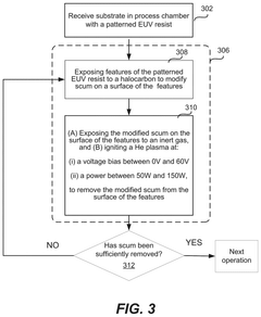
EUV metallic resist performance enhancement via additives
PatentPendingUS20240377735A1
Innovation
- Incorporating additives such as high boiling point solvents, photo acid generators, photo base generators, quenchers, photo decomposed bases, thermal acid generators, and photo sensitivity cross-linkers into the metallic photoresist materials to enhance their shelf life and CD control, specifically targeting the instability and variability issues in metallic resists.
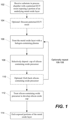
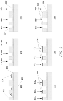
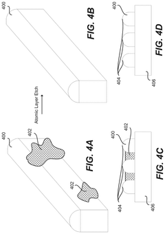
Atomic layer etch and selective deposition process for extreme ultraviolet lithography resist improvement
PatentPendingUS20240429045A1
Innovation
- The method involves descumming, divot filling, and protecting EUV resists by treating the substrate with halogen-containing plasmas, selectively depositing silicon-containing precursors, and forming silicon oxide caps or amorphous carbon caps to enhance etch selectivity and smoothness, using techniques like atomic layer etching and plasma processing.
Environmental Impact of EUV Resist Materials
The environmental impact of EUV resist materials represents a critical consideration in semiconductor manufacturing processes. These specialized photoresist formulations contain complex chemical compounds that may pose significant environmental and health risks if not properly managed throughout their lifecycle. Traditional photoresists have established environmental profiles, but EUV resists introduce novel components with potentially different environmental footprints.
Metal-containing EUV resists, particularly those incorporating tin, antimony, or other heavy metals, present unique environmental challenges. These metals can persist in the environment, potentially contaminating water systems and soil when improperly disposed. The manufacturing processes for these materials also require energy-intensive purification steps and specialized handling protocols to prevent environmental release.
Waste management for EUV resist materials demands sophisticated approaches. During semiconductor manufacturing, significant volumes of resist are removed during development and stripping processes, creating waste streams containing partially reacted compounds and additives. Current industry practices include chemical neutralization, incineration, and specialized waste treatment, though the efficacy of these methods for newer EUV resist formulations requires ongoing assessment.
Regulatory frameworks governing EUV resist materials vary globally, creating compliance challenges for international semiconductor manufacturers. The European Union's REACH regulations and similar initiatives in Asia and North America impose strict reporting and management requirements for potentially hazardous chemicals used in these formulations. As EUV lithography adoption accelerates, regulatory scrutiny of these materials is expected to intensify.
Industry initiatives are emerging to develop more environmentally sustainable EUV resist materials. Research directions include biodegradable polymer platforms, reduced metal content formulations, and closed-loop recycling systems for resist recovery. Several leading semiconductor materials suppliers have established sustainability programs specifically targeting photoresist environmental impact reduction, with measurable goals for reducing carbon footprints and hazardous waste generation.
The environmental lifecycle assessment of EUV resists must consider not only direct impacts but also indirect effects, including energy consumption during manufacturing and transportation. Preliminary studies suggest that while EUV lithography may offer process simplification benefits, the specialized nature of its resist materials may offset some environmental gains through increased material purification and handling requirements.
Cost-Performance Analysis of EUV Implementation
The implementation of Extreme Ultraviolet (EUV) lithography represents a significant financial investment for semiconductor manufacturers, necessitating thorough cost-performance analysis. Initial EUV scanner costs range from $120-150 million per unit, substantially higher than traditional immersion lithography tools at $40-60 million. This capital expenditure creates a considerable barrier to entry for smaller manufacturers and impacts the overall economics of chip production.
Beyond equipment costs, EUV implementation requires extensive facility modifications. Clean room specifications must be enhanced to accommodate the more stringent environmental controls needed for EUV processes, particularly for contact and via layers where defectivity control is critical. Infrastructure upgrades for power, cooling, and vacuum systems add approximately 15-20% to the base equipment cost.
Operational expenses present another significant cost factor. EUV systems consume substantially more power than conventional lithography tools, with estimates suggesting 500-700 kW per system compared to 100-200 kW for immersion lithography. Additionally, the specialized EUV light source requires regular maintenance and replacement of costly components, including laser-produced plasma systems and collector optics.
Against these costs, performance benefits must be carefully weighed. EUV enables significant process simplification for contact and via layers, reducing multi-patterning steps required with conventional lithography. Analysis indicates that for nodes below 7nm, EUV can reduce the total process steps by 20-30%, translating to cycle time improvements of 15-25% for critical layers.
Yield improvements represent another crucial performance metric. Current data suggests that properly optimized EUV resist processes can achieve 10-15% better yields for contact and via layers compared to multi-patterning approaches, primarily through reduced pattern placement errors and improved critical dimension uniformity.
Return on investment calculations indicate that despite high initial costs, EUV implementation becomes economically viable at high production volumes. For fabs producing more than 40,000 wafer starts per month, the break-even point typically occurs within 3-4 years. However, for lower volume production, the economic justification remains challenging, suggesting that EUV adoption will continue to be concentrated among larger semiconductor manufacturers with sufficient scale to absorb the substantial investment.
Unlock deeper insights with Patsnap Eureka Quick Research — get a full tech report to explore trends and direct your research. Try now!
Generate Your Research Report Instantly with AI Agent
Supercharge your innovation with Patsnap Eureka AI Agent Platform!