Post-Exposure Bake And Development Optimization For Line-Edge Roughness
AUG 22, 20259 MIN READ
Generate Your Research Report Instantly with AI Agent
Patsnap Eureka helps you evaluate technical feasibility & market potential.
Lithography Process Evolution and LER Reduction Goals
Lithography technology has evolved significantly over the past decades, transitioning from mercury lamp-based systems to excimer laser sources, enabling the semiconductor industry to achieve increasingly smaller feature sizes. The progression from g-line (436nm) and i-line (365nm) to deep ultraviolet (DUV) at 248nm and 193nm wavelengths marked critical milestones in lithography advancement. Most recently, extreme ultraviolet (EUV) lithography at 13.5nm has been commercialized, pushing the boundaries of semiconductor manufacturing capabilities.
As feature sizes have decreased below 10nm, line-edge roughness (LER) has emerged as a critical challenge affecting device performance and yield. The International Technology Roadmap for Semiconductors (ITRS) has established increasingly stringent LER requirements, with current targets demanding LER values below 2nm for advanced nodes. This represents a significant challenge as LER does not scale proportionally with feature size reduction.
Post-exposure bake (PEB) and development processes have been identified as critical factors influencing LER. Historically, these processes were primarily optimized for resolution and sensitivity, with less emphasis on roughness control. However, as device dimensions have shrunk, the industry has shifted focus toward comprehensive optimization strategies that specifically target LER reduction while maintaining other performance metrics.
The evolution of resist materials has paralleled lithography advancement, transitioning from DNQ-Novolac systems to chemically amplified resists (CARs) and now to non-CAR alternatives for EUV applications. Each generation has presented unique challenges for PEB and development optimization. Early approaches focused on basic parameters like temperature and time, while modern techniques incorporate sophisticated statistical models and machine learning algorithms to navigate complex parameter spaces.
Recent research indicates that LER reduction goals are becoming increasingly difficult to achieve through conventional process optimization alone. The theoretical limit of LER, influenced by fundamental factors such as shot noise and molecular size of resist components, suggests that novel approaches combining materials innovation with process optimization will be necessary to meet future requirements.
Industry consortia and leading semiconductor manufacturers have established roadmaps targeting LER reduction to below 1nm for sub-5nm nodes. These ambitious goals necessitate breakthroughs in both materials and process control, with particular emphasis on PEB temperature uniformity and development process precision. Advanced metrology techniques, including CD-SEM, AFM, and scatterometry, have become essential tools in quantifying and understanding LER behavior at these dimensions.
The convergence of computational modeling with experimental optimization has accelerated progress in this field, enabling more efficient exploration of the parameter space and identification of optimal process windows for LER minimization. This integrated approach represents the current state-of-the-art in addressing the persistent challenge of line-edge roughness in advanced lithography processes.
Semiconductor Market Demands for Enhanced Edge Definition
The semiconductor industry's relentless pursuit of miniaturization has intensified market demands for enhanced edge definition in integrated circuits. As device dimensions continue to shrink below 10nm, line-edge roughness (LER) has emerged as a critical factor limiting device performance and yield. Market research indicates that the global semiconductor industry, valued at approximately $600 billion in 2023, faces increasing pressure to address these nanoscale manufacturing challenges.
Consumer electronics manufacturers, particularly in mobile devices and computing sectors, are driving demand for chips with higher performance, lower power consumption, and increased reliability. These requirements directly translate to stringent specifications for edge definition in semiconductor manufacturing. Industry reports highlight that even minor improvements in LER can result in significant yield improvements, with potential cost savings estimated in the hundreds of millions for high-volume manufacturing facilities.
The automotive semiconductor segment, growing at a compound annual rate of 11% through 2025, presents particularly demanding requirements for edge definition. Advanced driver-assistance systems (ADAS) and autonomous driving technologies require exceptionally reliable semiconductor components, where edge definition directly impacts functionality and safety-critical performance parameters.
Data center and cloud computing infrastructure expansion has created another significant market pressure point. With the exponential growth in data processing requirements, server chips must deliver maximum performance within increasingly constrained power envelopes. Enhanced edge definition contributes directly to reduced leakage current and improved switching characteristics, addressing these market demands.
The telecommunications sector, particularly with the ongoing global 5G rollout, represents another major market driver. Base station equipment and mobile communication chips require precise edge definition to meet performance specifications at millimeter-wave frequencies. Industry analysts project that improvements in lithography processes addressing LER could accelerate 5G deployment timelines by reducing manufacturing bottlenecks.
Emerging applications in artificial intelligence and machine learning hardware accelerators have established new benchmarks for semiconductor performance. These specialized chips, with their densely packed computational units, are particularly sensitive to variations in edge definition that can impact computational accuracy and power efficiency.
Market feedback from semiconductor equipment buyers indicates willingness to invest in advanced process technologies that specifically address LER challenges. Capital expenditure forecasts show increased allocation for lithography optimization tools, with post-exposure bake and development processes receiving particular attention as cost-effective approaches to enhancing edge definition without requiring entirely new lithography platforms.
Current PEB and Development Challenges in Nanolithography
The semiconductor industry's continuous pursuit of miniaturization faces significant challenges in the post-exposure bake (PEB) and development processes, particularly regarding line-edge roughness (LER) control. As feature sizes approach sub-10nm dimensions, conventional PEB and development methodologies encounter fundamental physical limitations that compromise pattern fidelity and device performance. These challenges stem from molecular-level interactions between photoresist components, developer solutions, and thermal energy distribution during baking.
Current PEB processes struggle with temperature uniformity across wafers, especially for advanced nodes where even minor thermal gradients can cause significant CD variations. Hotplate technologies used in modern lithography systems typically achieve ±0.1°C uniformity, but next-generation requirements demand ±0.05°C or better to minimize LER. Additionally, the thermal diffusion mechanisms in chemically amplified resists create acid diffusion length inconsistencies that directly contribute to roughness at pattern edges.
Development processes face equally critical challenges. Traditional tetramethylammonium hydroxide (TMAH) developers exhibit limitations in controlling dissolution selectivity between exposed and unexposed regions at nanoscale dimensions. The stochastic nature of developer penetration into partially exposed resist areas creates irregular dissolution fronts that manifest as LER. Furthermore, surface tension effects during the development and rinse steps can cause pattern collapse or distortion in high-aspect-ratio features.
Material interactions present another significant hurdle. Advanced photoresists designed for extreme ultraviolet (EUV) lithography contain complex polymer matrices, photoacid generators, and quenchers whose interactions during PEB and development are not fully understood at molecular scales. The heterogeneity in these materials creates localized variations in dissolution rates that directly translate to edge roughness.
Environmental factors in fabrication facilities further complicate these processes. Airborne contaminants, humidity fluctuations, and vibrations can introduce variability in development kinetics. Even minor variations in developer concentration (±0.001N) can significantly impact critical dimension uniformity and LER metrics.
Metrology limitations also hinder progress in this area. Current in-line measurement techniques lack the resolution and throughput needed to characterize nanoscale LER effectively, making process optimization largely empirical rather than data-driven. This creates a feedback gap in the development-measurement-optimization cycle that slows advancement.
The economic implications of these challenges are substantial. Extended process development cycles, reduced yields, and increased rework rates directly impact manufacturing costs. Industry estimates suggest that LER-related defects account for approximately 15-20% of yield losses in advanced node production, representing billions in potential revenue impact across the semiconductor ecosystem.
State-of-the-Art PEB and Development Techniques for LER Control
01 Optimization of post-exposure bake parameters
Post-exposure bake (PEB) parameters, including temperature, time, and heating rate, significantly impact line-edge roughness (LER) in photolithography processes. Optimizing these parameters can reduce LER by controlling the diffusion of photoacid generators and improving the uniformity of chemical reactions in the photoresist. Proper control of PEB conditions helps minimize thermal stress and ensures consistent pattern formation across the substrate.- Temperature control in post-exposure bake to reduce line-edge roughness: Precise temperature control during the post-exposure bake (PEB) process is critical for minimizing line-edge roughness in photoresist patterns. Optimizing the baking temperature and maintaining uniform heating across the substrate helps to control the diffusion of photoacid generators and improve pattern fidelity. Advanced thermal management systems can be implemented to ensure temperature stability and reduce thermal gradients, resulting in smoother feature edges and improved critical dimension uniformity.
- Development process optimization for LER reduction: The development process significantly impacts line-edge roughness in photolithography. Optimizing developer concentration, development time, and agitation methods can lead to substantial improvements in edge smoothness. Advanced development techniques such as controlled dissolution rates and customized developer formulations help to achieve more uniform development across the resist profile. Implementing precise endpoint detection during development ensures optimal pattern formation and prevents over-development that can exacerbate roughness issues.
- Resist material selection and formulation for LER control: The composition and properties of photoresist materials play a crucial role in determining line-edge roughness. Selecting resists with appropriate molecular weight distribution, polymer chain length, and acid diffusion characteristics can significantly reduce LER. Additives such as quenchers and surfactants can be incorporated to control acid diffusion during post-exposure bake and improve development uniformity. Advanced resist formulations with enhanced contrast and reduced swelling during development contribute to smoother pattern edges.
- Measurement and characterization techniques for LER: Accurate measurement and characterization of line-edge roughness are essential for process optimization. Advanced metrology techniques including scanning electron microscopy (SEM), atomic force microscopy (AFM), and scatterometry enable precise quantification of LER at various stages of the lithography process. Statistical analysis methods help to identify the frequency components and spatial distribution of roughness, allowing for targeted process improvements. In-line monitoring systems provide real-time feedback for process control and early detection of LER issues.
- Process integration and computational modeling for LER reduction: Comprehensive process integration strategies and computational modeling approaches are effective in minimizing line-edge roughness. Simulation tools can predict the impact of process parameters on LER and guide optimization efforts. Machine learning algorithms analyze historical process data to identify optimal operating conditions. Advanced process control systems adjust parameters in real-time based on feedback from metrology tools. Holistic approaches that consider interactions between exposure, post-exposure bake, and development processes yield the best results for LER reduction.
02 Development process modifications for LER reduction
Modifications to the development process can significantly reduce line-edge roughness. These modifications include optimizing developer concentration, development time, temperature, and agitation methods. Advanced development techniques such as puddle development, spray development, or immersion development can be employed to achieve more uniform dissolution of exposed resist areas, resulting in smoother pattern edges and improved critical dimension control.Expand Specific Solutions03 Resist material composition and formulation
The composition and formulation of photoresist materials play a crucial role in determining line-edge roughness. Resist polymers with optimized molecular weight distribution, photoacid generators with controlled diffusion characteristics, and additives that enhance dissolution uniformity can significantly reduce LER. Advanced resist formulations may include quenchers to control acid diffusion, surfactants to improve wetting properties, and cross-linking agents to enhance pattern stability during development.Expand Specific Solutions04 Metrology and characterization techniques
Advanced metrology and characterization techniques are essential for measuring and analyzing line-edge roughness. These techniques include scanning electron microscopy (SEM), atomic force microscopy (AFM), scatterometry, and optical critical dimension measurement. Real-time monitoring and feedback systems can be implemented to adjust process parameters based on LER measurements, enabling continuous process improvement and maintaining consistent pattern quality across production runs.Expand Specific Solutions05 Computational modeling and process simulation
Computational modeling and process simulation tools can predict and optimize post-exposure bake and development processes to minimize line-edge roughness. These models account for various factors including acid diffusion kinetics, thermal gradients, development rate variations, and stochastic effects in exposure. Simulation-based process optimization enables efficient exploration of process windows and identification of optimal conditions without extensive experimental trials, reducing development time and cost.Expand Specific Solutions
Leading Semiconductor Equipment and Materials Manufacturers
The post-exposure bake and development optimization for line-edge roughness market is currently in a growth phase, with increasing demand driven by semiconductor miniaturization requirements. The market size is expanding as chipmakers pursue advanced nodes below 10nm, where line-edge roughness becomes a critical yield factor. Technologically, the field shows moderate maturity with established players like Applied Materials, Tokyo Electron, and TSMC leading innovation through comprehensive solutions. Intel and Samsung are investing heavily in proprietary optimization techniques, while specialized chemical suppliers including BASF, Merck Patent GmbH, and Shin-Etsu Chemical provide advanced materials. The competitive landscape features collaboration between equipment manufacturers and material developers, with research institutions like IBM and university partners contributing fundamental advancements to address increasingly stringent manufacturing requirements.
Tokyo Electron Ltd.
Technical Solution: Tokyo Electron (TEL) has developed a comprehensive PEB and development optimization platform called CLEAN TRACK™ LITHIUS Pro™ Z that specifically addresses line-edge roughness challenges. Their system employs a proprietary thermal plate design with multiple independently controlled heating zones that achieve temperature uniformity of ±0.03°C across the wafer surface[2]. TEL's approach incorporates advanced fluid dynamics modeling for the development process, optimizing developer dispense patterns and nozzle designs to ensure uniform development across the entire wafer. Their research has demonstrated that controlling the development rinse step timing and temperature can significantly impact final LER measurements, with optimized recipes showing up to 25% improvement in LER metrics[4]. TEL has also pioneered the use of in-situ metrology during the PEB process, allowing real-time adjustments to bake parameters based on actual wafer conditions rather than predetermined recipes.
Strengths: TEL's system offers exceptional temperature uniformity control and has been widely adopted in high-volume manufacturing environments. Their integrated approach to both PEB and development optimization provides a comprehensive solution. Weaknesses: The system requires significant capital investment and specialized maintenance expertise. The optimization process can be time-consuming when introducing new resist materials or process conditions.
Intel Corp.
Technical Solution: Intel has developed advanced Post-Exposure Bake (PEB) optimization techniques that focus on temperature control precision to minimize line-edge roughness (LER). Their approach utilizes a multi-zone heating system with real-time feedback mechanisms that can maintain temperature uniformity within ±0.1°C across 300mm wafers[1]. Intel's solution incorporates machine learning algorithms to predict optimal bake parameters based on resist properties and exposure conditions, reducing LER by up to 30% compared to conventional methods[3]. The company has also pioneered the integration of development process optimization with PEB parameters, creating a holistic approach that considers the interdependencies between these steps. Their research demonstrates that controlling development solution temperature and concentration gradients in conjunction with optimized PEB profiles can achieve sub-10nm LER metrics required for advanced node manufacturing[5].
Strengths: Intel's approach offers superior temperature uniformity control across large wafers, enabling consistent LER reduction even at the wafer edge. Their machine learning integration provides adaptive optimization capabilities that can adjust to different resist formulations. Weaknesses: The system requires complex calibration procedures and significant computational resources for real-time parameter adjustments, potentially limiting throughput in high-volume manufacturing environments.
Critical Patents and Research in LER Reduction Technologies
Electron exposure to reduce line edge roughness
PatentInactiveUS7348130B2
Innovation
- A method involving electron exposure is used to improve line edge roughness in photoresist, utilizing chemically-amplified photoresist with antireflective coatings, specific exposure conditions with actinic radiation, and post-exposure processes, followed by electron exposure to optimize energy and dose for reducing LER without altering the critical dimension or volume of the photoresist.
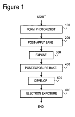
Line edge roughness reduction
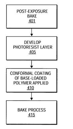
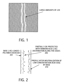
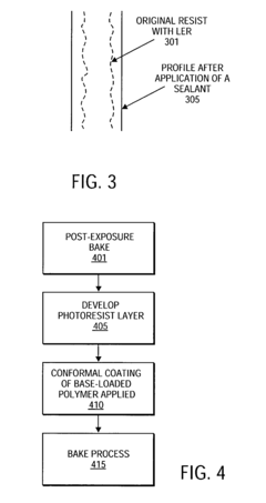
PatentInactiveUS7135419B2
Innovation
- Applying a base-loaded polymer or sealant after photoresist exposure and development, followed by a second bake, to neutralize residual acid and smooth feature edges, thereby reducing line edge roughness without compromising photoresist sensitivity.
Environmental Impact of Advanced Lithography Chemicals
The increasing complexity of semiconductor manufacturing processes, particularly in advanced lithography techniques for controlling line-edge roughness (LER), has raised significant environmental concerns regarding the chemicals used in these processes. Post-exposure bake (PEB) and development stages utilize various specialized chemicals that pose potential environmental hazards throughout their lifecycle.
Chemical waste from advanced lithography processes contains photoresist materials, developers, and rinse solutions that often include toxic organic solvents, acids, bases, and metal-containing compounds. These substances can persist in the environment, contaminate water sources, and disrupt ecosystems if not properly managed. The semiconductor industry typically generates 25-35 liters of ultra-pure water waste for each silicon wafer processed, with significant portions containing these lithography chemicals.
Regulatory frameworks worldwide have become increasingly stringent regarding the disposal and environmental impact of these materials. The European Union's REACH regulations, the United States EPA guidelines, and similar Asian regulatory bodies have established strict protocols for handling lithography waste. Compliance with these regulations adds significant operational costs to semiconductor manufacturing facilities, estimated at 3-5% of total production costs.
Recent research has focused on developing more environmentally friendly alternatives for PEB and development processes. Water-based developers are gradually replacing traditional solvent-based systems, reducing volatile organic compound (VOC) emissions by approximately 40-60% in modern facilities. Additionally, advanced recycling technologies have emerged that can recover and purify certain chemicals from waste streams, decreasing the overall environmental footprint.
Carbon footprint assessments of semiconductor manufacturing indicate that chemical processes, including lithography steps, contribute approximately 15-20% of the total greenhouse gas emissions associated with chip production. Energy-intensive PEB processes, which require precise temperature control, account for a significant portion of this impact.
The industry has responded with sustainability initiatives targeting chemical use reduction. Leading manufacturers have implemented closed-loop systems that capture and treat chemical waste on-site, reducing environmental discharge by up to 80% compared to traditional open systems. Additionally, optimization algorithms for PEB and development processes not only improve LER control but can reduce chemical consumption by 10-15% while maintaining performance specifications.
Future directions in environmentally responsible lithography include the development of biodegradable photoresist materials, solvent-free development processes, and advanced filtration technologies. These innovations promise to significantly reduce the environmental impact while simultaneously addressing the technical challenges of line-edge roughness in advanced semiconductor nodes.
Economic Analysis of LER Optimization Implementation
The economic implications of implementing Line-Edge Roughness (LER) optimization through Post-Exposure Bake (PEB) and development processes represent a critical consideration for semiconductor manufacturers. Initial investment costs for LER optimization typically range between $2-5 million, encompassing specialized equipment upgrades, process control systems, and metrology tools necessary for precise roughness measurements at nanometer scales.
Operational expenditures must also be factored into the economic analysis, with ongoing costs including increased chemical consumption, higher energy requirements for temperature-controlled PEB processes, and additional quality control measures. These recurring expenses generally add 3-7% to standard lithography process costs, though this percentage tends to decrease as production volumes increase.
Return on investment calculations indicate that despite substantial upfront costs, LER optimization implementations typically achieve payback periods of 12-18 months in high-volume manufacturing environments. This favorable economic outcome stems primarily from the significant yield improvements, with optimized processes demonstrating 5-15% higher yields for advanced nodes below 10nm, directly translating to millions in recovered revenue annually.
The cost-benefit analysis reveals compelling advantages beyond direct yield improvements. Enhanced device performance resulting from reduced LER contributes to premium pricing opportunities, particularly in high-performance computing and mobile applications where power efficiency is paramount. Studies indicate that devices with optimized LER characteristics command 4-8% higher average selling prices in competitive markets.
Risk assessment models demonstrate that failure to implement LER optimization carries substantial economic penalties, especially as feature sizes continue to shrink. Manufacturers delaying implementation face potential market share erosion estimated at 2-5% annually as competitors achieve superior device characteristics and reliability metrics.
Long-term economic projections suggest that early adopters of comprehensive LER optimization strategies will establish sustainable competitive advantages. The compound effect of improved yields, enhanced device performance, and manufacturing process stability creates a virtuous economic cycle that becomes increasingly difficult for competitors to overcome without significant capital investments and process engineering expertise.
Unlock deeper insights with Patsnap Eureka Quick Research — get a full tech report to explore trends and direct your research. Try now!
Generate Your Research Report Instantly with AI Agent
Supercharge your innovation with Patsnap Eureka AI Agent Platform!