Integration Of EUV Resists In Gate-All-Around And Backside Power Delivery
AUG 22, 20259 MIN READ
Generate Your Research Report Instantly with AI Agent
Patsnap Eureka helps you evaluate technical feasibility & market potential.
EUV Resist Technology Evolution and Objectives
Extreme Ultraviolet (EUV) lithography represents a revolutionary advancement in semiconductor manufacturing, enabling the continuation of Moore's Law beyond the limitations of traditional optical lithography. The evolution of EUV resist technology began in the early 2000s when semiconductor industry leaders recognized the need for next-generation lithography solutions to achieve sub-10nm feature sizes. Initial EUV resist formulations faced significant challenges including sensitivity, resolution, and line edge roughness—often referred to as the "triangle of death" in resist development.
The first generation of EUV resists evolved from traditional chemically amplified resists (CARs) used in 193nm lithography, modified to accommodate the 13.5nm wavelength of EUV light. These early formulations required exposure doses exceeding 30-50 mJ/cm², making them impractical for high-volume manufacturing due to throughput limitations. By 2010-2015, significant improvements in resist chemistry led to the development of second-generation resists with enhanced sensitivity (15-25 mJ/cm²) while maintaining acceptable resolution.
The period from 2015-2020 marked a critical transition as EUV lithography moved from research to production environments. During this phase, metal-oxide based resists emerged as promising alternatives to traditional organic resists, offering improved etch resistance and pattern transfer capabilities essential for advanced node manufacturing. Inorganic resist platforms demonstrated superior performance in line edge roughness control, a critical factor for Gate-All-Around (GAA) architectures where dimensional precision directly impacts transistor performance.
Current technological objectives for EUV resists focus on addressing the specific requirements of GAA transistor fabrication and backside power delivery integration. These advanced architectures demand unprecedented levels of pattern fidelity, with sub-5nm critical dimensions and minimal defectivity. Specifically, EUV resists must achieve exposure sensitivity below 20 mJ/cm², resolution capability of 8nm half-pitch or better, and line edge roughness under 2nm to meet the stringent requirements of GAA structures.
Looking forward, the industry aims to develop EUV resist technologies that can enable high-aspect-ratio patterning with minimal pattern collapse—a crucial requirement for the complex 3D structures in GAA transistors. Additionally, resist materials must demonstrate compatibility with subsequent process steps in backside power delivery schemes, including metal deposition and chemical-mechanical planarization. The ultimate objective is to create resist platforms that can simultaneously address sensitivity, resolution, roughness, and process integration challenges while maintaining economic viability for high-volume manufacturing environments.
Market Demand Analysis for Advanced Node Semiconductor Processes
The semiconductor industry is witnessing unprecedented demand for advanced node processes, driven primarily by the exponential growth in data processing requirements across multiple sectors. The integration of EUV resists in Gate-All-Around (GAA) architectures and Backside Power Delivery Network (BSPDN) technologies represents a critical advancement for sub-3nm nodes, addressing the increasing complexity of chip designs and performance requirements.
Market research indicates that the global semiconductor foundry market is projected to reach $150 billion by 2027, with advanced nodes (7nm and below) accounting for approximately 40% of this value. The demand for these advanced processes is primarily fueled by high-performance computing, artificial intelligence, 5G infrastructure, and autonomous systems that require greater transistor density and power efficiency.
The transition from FinFET to GAA architecture, coupled with the implementation of BSPDN, is creating significant market opportunities for EUV resist manufacturers. Industry analysts report that the EUV lithography materials market is growing at a compound annual growth rate of 26%, reflecting the accelerating adoption of EUV technology in advanced semiconductor manufacturing.
Major semiconductor manufacturers including TSMC, Samsung, and Intel have announced aggressive roadmaps for implementing GAA and BSPDN technologies in their sub-3nm nodes. These companies are collectively investing over $300 billion in capacity expansion and R&D over the next five years, with a substantial portion dedicated to advanced lithography solutions.
Customer requirements are evolving rapidly, with increasing emphasis on resist materials that can deliver higher resolution, lower line edge roughness, and improved sensitivity. The market is particularly demanding EUV resists that can support the complex patterning requirements of GAA structures while maintaining compatibility with the thermal and chemical processes involved in BSPDN integration.
Regional market analysis reveals that East Asia continues to dominate the advanced semiconductor manufacturing landscape, accounting for over 70% of global capacity. However, significant investments in the United States and Europe, supported by government initiatives like the CHIPS Act and European Chips Act, are expected to diversify the geographical distribution of advanced node manufacturing capabilities.
The market for specialized equipment and materials supporting EUV lithography in advanced node processes is experiencing particularly strong growth, with suppliers reporting order backlogs extending beyond 18 months. This supply-demand imbalance is creating premium pricing opportunities for companies with proven solutions for EUV resist integration in GAA and BSPDN architectures.
Current Challenges in EUV Resist Integration for GAA and BSPD
The integration of Extreme Ultraviolet (EUV) lithography resists into advanced semiconductor architectures such as Gate-All-Around (GAA) and Backside Power Delivery (BSPD) faces significant technical hurdles that impede widespread adoption. Current EUV resists exhibit pattern collapse issues at sub-10nm feature sizes, particularly problematic for the complex three-dimensional structures required in GAA transistors. The high aspect ratio features in these architectures create mechanical instability during development processes, resulting in yield-limiting defects.
Resolution limitations present another major challenge, as current EUV resists struggle to consistently achieve the 3-5nm resolution needed for advanced node GAA implementations. This is exacerbated by line edge roughness (LER) and line width roughness (LWR) issues that become increasingly problematic at smaller dimensions, directly impacting device performance and reliability.
Sensitivity trade-offs continue to plague EUV resist development, with the fundamental conflict between sensitivity, resolution, and line edge roughness forming an apparently unbreakable "triangle of death." Higher sensitivity resists typically sacrifice resolution or pattern fidelity, while high-resolution formulations often require prohibitively high exposure doses that reduce throughput and increase manufacturing costs.
Integration with multi-patterning schemes presents additional complexity, as EUV resists must maintain compatibility with the intricate process flows required for GAA and BSPD architectures. Overlay accuracy becomes increasingly critical, with requirements now pushing below 2nm for advanced nodes, stretching the capabilities of current metrology and process control systems.
Material compatibility issues arise when integrating EUV resists with the novel materials used in GAA and BSPD structures. Chemical interactions between resists and underlying films can lead to interfacial mixing, undercutting, or pattern degradation. Additionally, the outgassing characteristics of EUV resists can contaminate expensive EUV optics, necessitating careful material selection and qualification.
Process window limitations further constrain manufacturing viability, with current EUV resists demonstrating narrow process windows that complicate high-volume manufacturing. The depth of focus margins are particularly challenging for the topographical variations inherent in GAA structures, while exposure latitude constraints increase sensitivity to dose variations.
Defectivity remains a persistent concern, with EUV-specific defect mechanisms including stochastic failures, missing or bridging contacts, and metal residues that can cause electrical shorts. These defects become increasingly problematic at the densities required for advanced node GAA and BSPD implementations, directly impacting yield and reliability.
Current Integration Solutions for EUV Resists in Advanced Node Devices
01 Metal-containing EUV resist compositions
Metal-containing compounds are incorporated into EUV resist formulations to enhance absorption of EUV radiation and improve sensitivity. These metal elements, such as tin, antimony, or transition metals, provide higher EUV absorption cross-sections compared to traditional organic components. The metal can be incorporated through organometallic complexes, metal oxide nanoparticles, or metal-coordinated polymers, resulting in improved pattern resolution and reduced line edge roughness at lower exposure doses.- Metal-containing EUV resist compositions: Metal-containing compounds are incorporated into EUV resist formulations to enhance sensitivity and absorption of EUV radiation. These metal elements, such as tin, antimony, or transition metals, significantly improve pattern resolution and reduce line edge roughness due to their high EUV absorption cross-sections. The metal components can be integrated as organometallic complexes, metal oxide nanoparticles, or metal-coordinated polymers to achieve optimal lithographic performance.
- Chemically amplified resist systems for EUV lithography: Chemically amplified resist systems utilize photoacid generators (PAGs) that, upon EUV exposure, produce acids that catalyze multiple chemical reactions in the resist material. These systems typically contain a polymer matrix with acid-labile protecting groups, PAGs, and various additives to control diffusion and sensitivity. The chemical amplification mechanism allows for high sensitivity while maintaining the resolution requirements needed for advanced semiconductor manufacturing processes.
- Non-chemically amplified EUV resist materials: Non-chemically amplified resists for EUV lithography operate through direct photochemical reactions without acid amplification steps. These materials include chain-scission polymers, molecular glass resists, and metal oxide resists that undergo solubility changes directly upon EUV exposure. This approach offers advantages in terms of reduced post-exposure instability, improved line edge roughness, and better compatibility with smaller feature sizes required for advanced node semiconductor manufacturing.
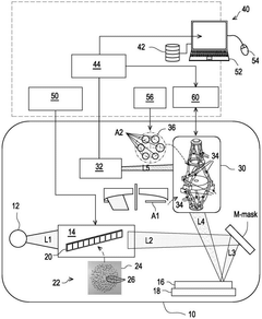
- EUV exposure systems and optimization techniques: EUV exposure systems require specialized optical configurations and process optimization techniques to maximize resist performance. These systems typically operate at 13.5nm wavelength and include reflective optics, vacuum environments, and precise dose control mechanisms. Process optimization techniques include focus-exposure matrix analysis, post-exposure bake optimization, and development process tuning to achieve the desired pattern fidelity, sensitivity, and line edge roughness characteristics.
- Novel additives and components for EUV resist formulations: Various additives and components are incorporated into EUV resist formulations to enhance performance characteristics. These include quenchers to control acid diffusion, sensitizers to improve quantum yield, nanoparticles to enhance sensitivity, and surfactants to improve coating uniformity. Advanced polymer architectures with tailored functional groups are also developed to achieve the optimal balance between sensitivity, resolution, line edge roughness, and pattern collapse resistance required for next-generation semiconductor devices.
02 Hybrid and multi-layer resist systems
Hybrid resist systems combine multiple functional components or layers to overcome limitations of single-layer resists. These systems may include a top imaging layer sensitive to EUV radiation and an underlying transfer layer, or incorporate both positive and negative tone mechanisms. Multi-layer approaches help manage pattern collapse issues while maintaining high resolution, and can incorporate different chemistries optimized for specific functions like acid generation, development contrast, or etch resistance.Expand Specific Solutions03 EUV resist development and processing techniques
Advanced development and processing techniques are crucial for EUV lithography performance. These include specialized developers, post-exposure bake optimization, and novel development methods like supercritical CO2 development. Process refinements such as controlled diffusion mechanisms, optimized development temperatures, and specialized rinse procedures help minimize pattern collapse and improve resolution while maintaining acceptable throughput in manufacturing environments.Expand Specific Solutions04 Chemical amplification and sensitivity enhancement
Chemical amplification mechanisms are optimized for EUV resists to achieve high sensitivity while maintaining resolution. These systems typically employ photoacid generators (PAGs) that create catalytic species upon EUV exposure, which then drive multiple chemical reactions during post-exposure processing. Advanced formulations incorporate specialized quenchers to control acid diffusion, custom-designed polymer matrices with tuned deprotection kinetics, and additives that enhance quantum yield to improve overall lithographic performance.Expand Specific Solutions05 EUV exposure systems and integration
EUV resist performance is closely tied to exposure system design and integration. Advanced EUV scanners operate at 13.5nm wavelength and require specialized optical systems, including reflective optics and vacuum environments. Resist formulations must be compatible with these systems and address challenges like outgassing, which can contaminate optical elements. Integration considerations include resist thickness optimization, substrate interactions, and compatibility with existing semiconductor manufacturing processes to enable high-volume manufacturing.Expand Specific Solutions
Leading Semiconductor Companies and Equipment Manufacturers Analysis
The integration of EUV resists in Gate-All-Around and Backside Power Delivery technologies represents an emerging frontier in semiconductor manufacturing, currently in the early growth phase. The market is expanding rapidly with projections exceeding $2 billion by 2025, driven by advanced node development. Leading semiconductor manufacturers like TSMC, Samsung, and Intel are at the forefront, with IBM demonstrating significant technical advancements. Equipment suppliers Applied Materials and ASML provide critical infrastructure, while specialized materials companies including AGC and Shanghai Sinyang develop advanced resist formulations. Research institutions like IMEC collaborate with industry players to overcome technical challenges in resist sensitivity, resolution, and pattern collapse, as the technology approaches commercial maturity for sub-3nm nodes.
Intel Corp.
Technical Solution: Intel has developed a comprehensive EUV resist integration strategy for their RibbonFET (Intel's version of GAA) technology and backside power delivery network (BSPDN). Their approach features chemically amplified resists specifically engineered for high-aspect-ratio GAA structures with reduced line edge roughness. Intel's EUV resist platform incorporates metal-oxide additives that enhance sensitivity while maintaining pattern fidelity at sub-7nm dimensions. For backside power delivery, Intel employs a specialized dual-damascene process compatible with their EUV resist system, enabling precise via formation and metallization. Their integration methodology includes advanced post-exposure processing techniques that optimize pattern transfer while minimizing defectivity. Intel's EUV resist technology incorporates specialized underlayers designed to enhance adhesion and reduce pattern collapse in the complex 3D structures required for GAA implementation, while their backside power delivery approach utilizes specialized dielectric materials compatible with their EUV process flow.
Strengths: Vertically integrated manufacturing capability allowing for customized resist formulations; extensive experience with advanced transistor architectures. Weaknesses: Historical challenges with process node transitions; complex integration requirements for their specific GAA implementation.
Taiwan Semiconductor Manufacturing Co., Ltd.
Technical Solution: TSMC has pioneered advanced EUV resist integration for Gate-All-Around (GAA) architectures, developing specialized resist formulations with enhanced sensitivity and resolution capabilities specifically optimized for their 3nm and 2nm process nodes. Their approach combines metal-oxide EUV resists with multi-patterning techniques to achieve sub-5nm features required for GAA structures. For backside power delivery, TSMC has implemented a comprehensive solution involving through-silicon vias (TSVs) and backside metallization processes compatible with their EUV resist systems. Their integration methodology includes specialized post-exposure bake processes that minimize pattern collapse while maintaining critical dimension uniformity across wafer-scale production. TSMC's EUV resist platform incorporates metal-organic compounds that enhance sensitivity while reducing line edge roughness to below 2nm, critical for GAA implementation.
Strengths: Industry-leading EUV lithography infrastructure with proven high-volume manufacturing capability; proprietary resist formulations optimized for GAA structures. Weaknesses: Higher production costs compared to traditional lithography approaches; requires significant capital investment for implementation.
Key Patents and Technical Innovations in EUV Resist Materials
EUV generating device
PatentActiveUS20190239328A1
Innovation
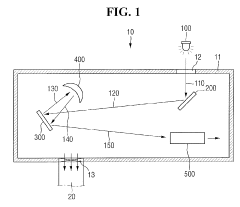
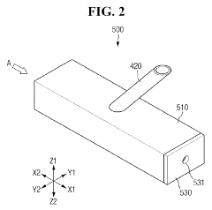
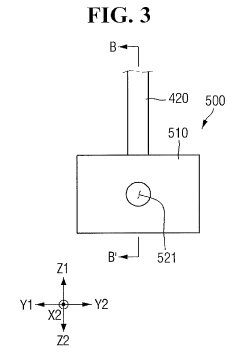
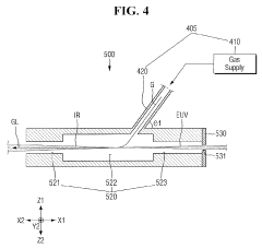
- The EUV generating device incorporates a gas cell with a light guide passage and a gas supply passage connected at an acute angle, directing the plasma reaction gas to interact with incident infrared laser pulses to generate EUV light, while minimizing the leftover gas along the EUV light path by releasing it towards the incident portion, thus maintaining high plasma density for generation and low density for emission.
System for extreme ultraviolet radiation actinic mask review
PatentActiveCN220553081U
Innovation
- A dedicated EUV actinic mask review system is designed, including a mask table, EUV illuminator, EUV imaging sensor and projection optical element box, all components are contained in a vacuum chamber, allowing the system to be adjusted in a vacuum state to perform Quick review.
Supply Chain Considerations for Advanced Lithography Materials
The supply chain for advanced lithography materials, particularly EUV resists required for Gate-All-Around (GAA) and Backside Power Delivery (BSPD) technologies, presents significant strategic considerations for semiconductor manufacturers. The global EUV resist market remains highly concentrated, with approximately 80% of production controlled by Japanese chemical companies including JSR, TOK, and Shin-Etsu Chemical.
This concentration creates potential vulnerabilities in the supply chain, especially as geopolitical tensions increase between major semiconductor manufacturing regions. The specialized nature of EUV resists for GAA and BSPD applications further narrows the supplier base, as these advanced node applications require materials with extremely precise properties and unprecedented performance characteristics.
Raw material sourcing represents another critical consideration. Key components for EUV resists include metal-organic compounds containing hafnium, zirconium, and tin, many of which have limited sources globally. The purification processes for these materials demand specialized equipment and expertise, creating additional supply chain bottlenecks that can impact production schedules for leading-edge devices.
Logistics and transportation of these sensitive materials present unique challenges. EUV resists require strict temperature control during shipping and storage, typically between 4-10°C, with specialized packaging to prevent contamination. Any disruption in the cold chain can render these expensive materials unusable, adding complexity to global distribution networks.
Inventory management strategies must evolve to accommodate the characteristics of these materials. Unlike conventional resists, EUV formulations often have shorter shelf lives (typically 6-9 months) and higher costs (approximately 5-7 times that of ArF resists), necessitating more sophisticated just-in-time delivery systems while maintaining sufficient safety stock to prevent production interruptions.
Regulatory compliance adds another layer of complexity. The chemical components in advanced EUV resists face increasing scrutiny under frameworks such as REACH in Europe and similar regulations in Asia and North America. Manufacturers must navigate a complex landscape of chemical registration requirements that can vary significantly between regions.
Vertical integration has emerged as a strategic response to these challenges. Leading semiconductor manufacturers are increasingly investing in joint ventures or direct partnerships with resist suppliers to ensure priority access to these critical materials. This trend represents a significant shift from the traditional arm's-length supplier relationships that characterized earlier technology nodes.
Environmental and Safety Implications of EUV Resist Processing
The integration of Extreme Ultraviolet (EUV) lithography resists in advanced semiconductor architectures such as Gate-All-Around (GAA) and Backside Power Delivery (BSPD) introduces significant environmental and safety considerations that must be addressed throughout the manufacturing process. EUV resists contain complex chemical compounds, including metal-organic materials and photoacid generators, which present unique challenges compared to traditional photoresists.
Chemical exposure risks constitute a primary concern in EUV resist processing environments. The metal-containing components in EUV resists, particularly tin and antimony compounds, can pose toxicity hazards if proper handling protocols are not implemented. Manufacturing facilities must establish rigorous exposure limits and monitoring systems to protect personnel from both acute and chronic health effects associated with these materials.
Waste management represents another critical environmental dimension of EUV resist processing. The semiconductor industry generates substantial quantities of chemical waste during lithography processes, with EUV resists contributing to this burden through developer solutions, rinse water, and resist stripping chemicals. Advanced treatment technologies, including precipitation methods and specialized filtration systems, are being deployed to capture metal components before discharge into municipal waste streams.
Energy consumption patterns for EUV lithography differ significantly from previous generation technologies. The high-power EUV light sources require substantial electricity inputs, contributing to the carbon footprint of semiconductor manufacturing. This energy intensity necessitates comprehensive life cycle assessments to quantify environmental impacts and identify optimization opportunities throughout the resist processing workflow.
Regulatory compliance frameworks for EUV resist handling continue to evolve globally. The European Union's REACH regulations, the United States EPA guidelines, and similar Asian regulatory structures impose increasingly stringent requirements on chemical management in semiconductor fabrication. Manufacturers must navigate this complex regulatory landscape while maintaining production efficiency and meeting technical performance targets.
Sustainable alternatives in resist chemistry represent a promising research direction. Development efforts focus on reducing metal content, decreasing toxicity profiles, and enhancing biodegradability without compromising lithographic performance. These green chemistry initiatives align with broader industry sustainability goals while potentially offering cost advantages through reduced waste treatment requirements.
Emergency response protocols specific to EUV resist incidents require specialized training and equipment. The unique chemical properties of these materials necessitate tailored containment strategies, neutralization approaches, and decontamination procedures to address accidental releases or exposures in the fabrication environment.
Unlock deeper insights with Patsnap Eureka Quick Research — get a full tech report to explore trends and direct your research. Try now!
Generate Your Research Report Instantly with AI Agent
Supercharge your innovation with Patsnap Eureka AI Agent Platform!