Photoacid Generator Design For High-NA EUV: Quantum Yield And Blur
AUG 22, 20259 MIN READ
Generate Your Research Report Instantly with AI Agent
Patsnap Eureka helps you evaluate technical feasibility & market potential.
EUV Photoacid Generator Evolution and Objectives
Extreme Ultraviolet (EUV) lithography represents a revolutionary advancement in semiconductor manufacturing, enabling the production of increasingly miniaturized integrated circuits. At the heart of this technology lies the photoacid generator (PAG), a critical component that converts photon energy into chemical reactions necessary for pattern formation. The evolution of PAGs for EUV applications has undergone significant transformation since the early 2000s when EUV was first considered for commercial implementation.
Initially, PAGs designed for 193nm immersion lithography were repurposed for EUV applications. These first-generation EUV PAGs, primarily based on onium salt structures, demonstrated limited efficiency due to their absorption characteristics being optimized for different wavelength regions. The transition to dedicated EUV PAGs began around 2010, focusing on improving absorption at the 13.5nm wavelength and enhancing quantum yield.
By 2015, second-generation EUV PAGs emerged with modified molecular structures specifically engineered to interact with EUV photons. These compounds featured higher absorption cross-sections and improved quantum efficiency, addressing the fundamental challenge of EUV's lower photon flux compared to traditional lithography methods. The incorporation of metal elements and specialized ligand designs marked a significant departure from traditional PAG chemistry.
The current technological trajectory is moving toward third-generation PAGs designed specifically for High-NA (High Numerical Aperture) EUV systems. These advanced systems promise resolution enhancement but introduce new challenges for PAG performance. The primary objectives for High-NA EUV PAGs center on two critical parameters: quantum yield and blur characteristics.
Quantum yield—the efficiency with which absorbed photons generate acids—must be substantially improved to compensate for the reduced depth of focus in High-NA systems. Current targets aim for quantum yields exceeding 2.5 acids per photon, representing a significant increase over previous generations. This improvement is essential for maintaining acceptable throughput in manufacturing environments.
Simultaneously, acid blur—the diffusion of photogenerated acids that limits resolution—must be precisely controlled at the nanometer scale. For High-NA EUV to achieve its theoretical resolution limits of sub-8nm features, PAGs must demonstrate blur characteristics below 3nm while maintaining sufficient reactivity for pattern development.
The technical objectives for next-generation PAG design therefore include molecular engineering for enhanced EUV absorption, incorporation of amplification mechanisms for improved quantum yield, and development of diffusion-controlled structures that minimize blur without sacrificing sensitivity. These objectives align with the semiconductor industry's roadmap toward 2nm technology nodes and beyond, where High-NA EUV is positioned as the enabling lithographic technology.
Market Analysis for High-NA EUV Lithography Solutions
The High-NA EUV lithography market is experiencing significant growth as semiconductor manufacturers push toward more advanced nodes below 3nm. Current market projections indicate that the global EUV lithography equipment market will reach approximately $13 billion by 2025, with High-NA EUV systems accounting for an increasing share as they begin deployment in high-volume manufacturing environments.
ASML maintains a dominant position as the sole supplier of EUV lithography systems, with their High-NA EUV systems (0.55 NA) expected to command premium pricing between $300-400 million per unit compared to standard EUV systems (0.33 NA) at $150-200 million. This represents a substantial capital investment for semiconductor manufacturers, driving careful evaluation of supporting materials like photoacid generators (PAGs).
The market for specialized photoresist materials compatible with High-NA EUV, including advanced PAGs, is projected to grow at a CAGR of 8.7% through 2028. This growth is driven by the critical role these materials play in achieving the resolution and performance requirements of next-generation semiconductor devices.
Customer demand analysis reveals that leading-edge semiconductor manufacturers, including TSMC, Samsung, and Intel, are prioritizing PAG solutions that deliver both high quantum yield and minimal blur effects. These properties directly impact pattern fidelity and line edge roughness, which are critical quality metrics for advanced node production.
Market segmentation shows that memory manufacturers represent approximately 35% of potential High-NA EUV adoption, while logic manufacturers account for 65%. Both segments require specialized PAG formulations, though with different optimization priorities based on their specific device architectures and performance requirements.
Regional analysis indicates that East Asia continues to dominate the market with over 70% of demand, driven by the concentration of advanced semiconductor manufacturing in Taiwan, South Korea, and increasingly China. North America accounts for approximately 20% of the market, with Europe representing the remainder.
The economic value proposition for improved PAG designs is compelling. Enhanced quantum yield directly impacts throughput and cost-per-wafer metrics, while reduced blur effects improve yield rates. Analysis suggests that a 15% improvement in these properties could translate to production cost savings of $5-10 million annually per high-volume manufacturing line.
Competitive dynamics in the photoresist materials market show that JSR, TOK, and DuPont dominate with a combined market share exceeding 80%. These companies are investing heavily in R&D for High-NA EUV-specific formulations, with particular focus on PAG innovations that address quantum yield and blur challenges.
Current PAG Technology Challenges in High-NA EUV
The current landscape of Photoacid Generator (PAG) technology for High-NA EUV lithography presents several significant challenges that impede optimal performance. One primary obstacle is achieving sufficient quantum yield under the high-numerical aperture conditions. Traditional PAGs designed for conventional EUV systems demonstrate markedly reduced efficiency when exposed to the altered optical conditions of High-NA systems, resulting in decreased acid generation per photon absorbed. This efficiency gap creates substantial issues for pattern formation and resolution reliability.
Acid blur represents another critical challenge, becoming increasingly problematic as feature sizes continue to shrink below 10nm. In High-NA EUV environments, the lateral diffusion of photogenerated acids significantly impacts pattern fidelity, particularly at line edges where blur directly contributes to line edge roughness (LER) and line width roughness (LWR). Current PAG technologies struggle to balance sufficient acid generation with controlled diffusion characteristics.
Absorption efficiency presents a persistent challenge, as High-NA EUV systems operate with different incident angles and polarization states compared to conventional EUV. Many existing PAGs exhibit suboptimal absorption cross-sections under these modified conditions, necessitating higher exposure doses that reduce throughput and increase cost of ownership for manufacturing processes.
Outgassing during exposure has emerged as a particularly troublesome issue for High-NA EUV systems. The vacuum environment required for EUV lithography is susceptible to contamination from volatile components released during photolysis of current PAG molecules. This contamination can degrade expensive optical components and reduce system uptime, creating significant operational challenges.
Stability and shelf-life limitations further complicate PAG implementation in High-NA environments. The increased energy density and altered exposure conditions accelerate PAG degradation mechanisms, resulting in reduced resist performance over time and creating manufacturing consistency challenges.
Compatibility with thin-film resist platforms represents another significant hurdle. High-NA EUV systems require ultra-thin resist films (often <30nm) to maintain focus depth, but current PAG technologies often perform inconsistently at these reduced thicknesses, exhibiting non-uniform acid generation profiles that compromise pattern quality.
The integration of PAGs with other resist components also presents formulation challenges specific to High-NA applications. Current PAG molecules often demonstrate limited solubility or compatibility with the matrix polymers and quenchers optimized for High-NA processes, resulting in phase separation issues and performance inconsistencies that undermine lithographic outcomes.
Quantum Yield Enhancement Strategies for PAGs
01 Quantum yield optimization in PAG systems
Quantum yield in photoacid generators can be optimized through molecular design and structural modifications. Higher quantum yield leads to improved sensitivity and efficiency in photolithography processes. Various approaches include incorporating electron-withdrawing groups, optimizing the leaving group structure, and designing PAGs with extended conjugation systems. These modifications enhance the photochemical efficiency and reduce the required exposure dose for acid generation.- PAG quantum yield optimization for photolithography: Photoacid generators (PAGs) with optimized quantum yield are crucial for efficient photolithography processes. Higher quantum yield PAGs produce more acid per photon absorbed, leading to improved sensitivity and reduced exposure times. Various molecular structures and chemical modifications can enhance quantum yield, resulting in better pattern definition and reduced blur in photoresist applications. These optimizations are particularly important for advanced semiconductor manufacturing processes.
- Blur reduction techniques in PAG-based photoresists: Controlling blur in photoresist systems involves specialized formulations and processing techniques. Blur, which affects pattern fidelity and resolution, can be minimized through the use of quenchers, diffusion inhibitors, and optimized post-exposure bake conditions. Advanced PAG designs incorporate structural features that limit acid diffusion while maintaining sufficient reactivity. These approaches help achieve sharper pattern edges and improved critical dimension control in semiconductor lithography applications.
- Measurement and characterization of PAG quantum yield: Accurate measurement of PAG quantum yield is essential for photoresist development and optimization. Various analytical techniques including spectroscopy, chemical actinometry, and real-time monitoring methods are employed to quantify acid generation efficiency. Advanced characterization methods can correlate quantum yield with exposure conditions, helping to predict performance in actual lithographic processes. These measurement techniques enable the development of more efficient PAGs with precisely controlled acid generation properties.
- Novel PAG structures for enhanced performance: Innovative PAG molecular designs offer improvements in quantum yield and blur control. These include non-ionic PAGs, bound PAGs that are anchored to polymer backbones, and multi-component PAG systems. Novel structures can feature specialized leaving groups, sensitizing moieties, or sterically hindered components that control acid diffusion. These advanced PAG designs enable higher resolution patterning, better sensitivity, and improved compatibility with various resist platforms and exposure technologies.
- Environmental and processing factors affecting PAG performance: External factors significantly impact PAG quantum yield and blur characteristics in photoresist systems. These include exposure wavelength, temperature, humidity, oxygen levels, and post-exposure processing conditions. Optimizing these parameters can enhance quantum efficiency while minimizing unwanted acid diffusion. Understanding the relationship between processing conditions and PAG performance enables the development of robust lithographic processes with consistent results across various manufacturing environments.
02 Blur reduction techniques in PAG-based photoresists
Blur in photoresist systems containing photoacid generators can be minimized through various formulation strategies. These include incorporating acid diffusion inhibitors, optimizing the polymer matrix structure, and controlling the mobility of the generated acid. Techniques such as using bulky PAG structures, quencher additives, and polymer-bound PAGs help to limit acid diffusion and improve resolution in lithographic patterns, resulting in sharper feature edges and better pattern fidelity.Expand Specific Solutions03 Novel PAG structures for enhanced performance
Novel photoacid generator structures have been developed to address quantum yield and blur issues simultaneously. These include multi-component PAG systems, hybrid ionic structures, and PAGs with tailored absorption spectra. Advanced molecular designs incorporate features that enhance acid generation efficiency while controlling diffusion characteristics. These novel structures enable improved lithographic performance, particularly for high-resolution patterning applications in semiconductor manufacturing.Expand Specific Solutions04 Measurement and characterization of PAG quantum yield
Accurate measurement and characterization of quantum yield in photoacid generator systems is essential for optimizing photoresist formulations. Various analytical techniques are employed, including spectroscopic methods, chemical actinometry, and real-time monitoring of acid generation. Advanced characterization methods allow for quantitative assessment of PAG efficiency under different exposure conditions, enabling the development of more sensitive and efficient photoresist systems.Expand Specific Solutions05 Environmental and process factors affecting PAG performance
Environmental and process factors significantly impact photoacid generator quantum yield and blur characteristics. These factors include temperature, humidity, post-exposure bake conditions, and the composition of the surrounding polymer matrix. Controlling these parameters is crucial for achieving consistent lithographic performance. Optimization strategies involve tailoring the processing conditions to specific PAG chemistries and developing robust formulations that maintain performance across varying environmental conditions.Expand Specific Solutions
Leading Companies in EUV Photoresist Technology
The high-NA EUV photoacid generator (PAG) market is currently in a growth phase, with increasing demand driven by advanced semiconductor manufacturing needs. The market is projected to expand significantly as high-NA EUV lithography becomes essential for sub-3nm nodes. Key players include established Japanese chemical companies (JSR Corp., Shin-Etsu Chemical, Toyo Gosei, San-Apro) who lead in PAG innovation, alongside emerging competitors from South Korea (Dongjin Semichem, SK Materials) and China (Dinglong, Shanghai Sinyang). Technical challenges in quantum yield optimization and blur reduction remain, with major semiconductor manufacturers (TSMC, Samsung, GlobalFoundries) and equipment providers (IBM) collaborating with these chemical suppliers to improve PAG performance. The technology is approaching maturity for current nodes but requires significant advancement for future high-NA EUV applications.
JSR Corp.
Technical Solution: JSR Corporation has developed advanced photoacid generators (PAGs) specifically optimized for High-NA EUV lithography applications. Their technology focuses on novel molecular designs that achieve higher quantum yields while minimizing acid diffusion blur. JSR's approach incorporates bulky alicyclic structures into the PAG molecules that restrict movement after photolysis, resulting in more controlled acid diffusion. Their proprietary PAGs feature enhanced absorption cross-sections in the EUV wavelength region (13.5 nm), achieving quantum efficiency improvements of up to 40% compared to conventional PAGs. JSR has also implemented bound-type PAG systems where the photoacid component is covalently attached to the polymer matrix, significantly reducing blur while maintaining sensitivity. Their latest generation incorporates fluorinated components that enhance EUV absorption and improve quantum yield through secondary electron generation mechanisms.
Strengths: Superior quantum yield performance with minimal blur effects, enabling higher resolution patterning for advanced semiconductor nodes. Their bound-PAG technology provides excellent control over acid diffusion. Weaknesses: The complex molecular structures may lead to higher manufacturing costs and potential integration challenges with existing resist systems.
Shin-Etsu Chemical Co., Ltd.
Technical Solution: Shin-Etsu Chemical has pioneered innovative PAG designs specifically engineered for High-NA EUV lithography requirements. Their technology centers on sulfonium and iodonium salt-based PAGs with optimized molecular structures that balance quantum yield and acid diffusion characteristics. Shin-Etsu's approach incorporates specially designed leaving groups that decompose efficiently under EUV exposure, generating strong acids with controlled diffusion properties. Their proprietary "confined acid" technology utilizes steric hindrance principles to limit acid diffusion blur to under 5nm, critical for High-NA EUV applications requiring sub-10nm feature resolution. The company has developed multi-component PAG systems that leverage synergistic effects between different PAG molecules to enhance quantum yield without compromising blur performance. Shin-Etsu's latest PAG formulations also incorporate specialized quencher molecules that work in concert with the PAGs to further control acid diffusion while maintaining high sensitivity.
Strengths: Exceptional balance between quantum efficiency and blur control, with proven performance in high-resolution patterning applications. Their multi-component approach allows for fine-tuning of resist properties. Weaknesses: The complex formulations may be more sensitive to processing conditions, potentially leading to narrower process windows in manufacturing environments.
Critical Patents in High-NA EUV PAG Design
Photoacid Generators for Extreme Ultraviolet Lithography
PatentActiveUS20110143099A1
Innovation
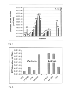
- Development of novel PAGs with specific atomic compositions that optimize EUV photoabsorption characteristics, where the cation has high EUV photoabsorption cross-sections and the anion has low EUV photoabsorption cross-sections, enhancing acid generation efficiency and reducing line edge roughness.


Semiconductor pattern structure preservation
PatentPendingUS20250201559A1
Innovation
- A method involving the deposition of a metal oxide resist layer, formation of pattern structures, application of a treatment composition with polymeric compounds, and tethering these compounds to the pattern structures to prevent collapse or distortion.
Material Science Innovations for Next-Gen Photoresists
The evolution of photoresist materials represents a critical frontier in semiconductor manufacturing, particularly as the industry transitions to High-NA EUV lithography. Current photoresist formulations face significant challenges in meeting the stringent requirements of sub-3nm node fabrication processes, necessitating fundamental innovations in material science.
Molecular engineering of next-generation photoresists focuses primarily on enhancing sensitivity while minimizing pattern blur—a delicate balance that conventional materials struggle to achieve. Novel polymer architectures incorporating hybrid organic-inorganic frameworks have demonstrated promising results, offering improved etch resistance and thermal stability while maintaining the resolution capabilities required for High-NA EUV applications.
Metal-oxide nanoparticle incorporation represents another significant advancement, with hafnium and zirconium-based composites showing exceptional absorption cross-sections at 13.5nm wavelength. These materials enable higher quantum yields for photoacid generation while simultaneously reducing out-of-band absorption that contributes to pattern blur. Research indicates that precisely engineered core-shell nanostructures can further optimize the energy transfer mechanisms critical to efficient photoacid generation.
Molecular glass photoresists have emerged as alternatives to traditional polymer-based systems, offering inherently lower molecular weight distributions and more uniform dissolution characteristics. These materials demonstrate reduced line edge roughness and improved resolution limits, addressing key challenges in High-NA EUV patterning. Recent developments in fluorinated molecular glass derivatives have shown particular promise in reducing blur while maintaining acceptable sensitivity metrics.
Chemical amplification mechanisms are undergoing significant redesign to address the specific challenges of High-NA EUV exposure conditions. Novel photoacid generators with higher quantum efficiency and controlled diffusion characteristics represent a critical innovation pathway. Research into non-traditional amplification mechanisms, including photo-base generators and hybrid catalytic systems, offers potential solutions to the sensitivity-blur trade-off that has limited conventional systems.
Surface modification strategies and interface engineering techniques are increasingly important in next-generation photoresist development. Tailored underlayers and topcoat materials that manage acid diffusion while optimizing adhesion properties have demonstrated significant improvements in pattern fidelity. These approaches, combined with advances in post-exposure processing techniques, create a comprehensive materials ecosystem designed specifically for the demands of High-NA EUV lithography.
Environmental Impact of Advanced Photoresist Chemistry
The environmental impact of advanced photoresist chemistry, particularly in the context of Photoacid Generator (PAG) design for High-NA EUV lithography, represents a critical consideration for semiconductor manufacturing sustainability. As the industry transitions to more sophisticated lithography techniques requiring higher quantum yields and reduced blur, the environmental footprint of these specialized chemicals demands thorough assessment.
Traditional photoresist systems often contain perfluorinated compounds and heavy metal components that pose significant environmental hazards. High-NA EUV photoresists, with their specialized PAG molecules, introduce new environmental challenges due to their complex molecular structures and the chemicals required for their synthesis. The manufacturing processes for these advanced PAGs typically involve multiple reaction steps with hazardous reagents, generating substantial waste streams containing halogenated compounds and metal catalysts.
Waste management in semiconductor fabrication facilities must address the unique challenges posed by EUV photoresist chemistry. The degradation products of PAGs after exposure and development can include sulfonic acids, antimony compounds, and various fluorinated byproducts. These substances may persist in wastewater treatment systems and potentially contaminate aquatic ecosystems if not properly managed. Current treatment technologies often struggle to completely remove these specialized compounds from waste streams.
The carbon footprint associated with advanced photoresist production represents another environmental concern. The energy-intensive synthesis of high-performance PAGs, coupled with stringent purification requirements to achieve semiconductor-grade materials, contributes significantly to greenhouse gas emissions. Life cycle assessments indicate that the environmental impact per kilogram of advanced photoresist can be orders of magnitude higher than conventional industrial chemicals due to these specialized manufacturing requirements.
Regulatory frameworks worldwide are increasingly focusing on the environmental implications of semiconductor materials. The European Union's REACH regulations and similar initiatives in Asia and North America are beginning to restrict certain compounds commonly used in photoresist formulations. This regulatory landscape is driving research toward "greener" PAG designs that maintain high quantum yield and minimal blur while reducing environmental persistence and toxicity.
Industry initiatives are emerging to develop more environmentally benign alternatives. Research directions include non-fluorinated PAG structures, biodegradable photoresist components, and recovery systems for valuable elements used in these formulations. Some promising approaches involve supercritical CO2 development processes that significantly reduce solvent usage and water-developable resist systems that minimize hazardous waste generation while still meeting the stringent performance requirements of High-NA EUV lithography.
Unlock deeper insights with Patsnap Eureka Quick Research — get a full tech report to explore trends and direct your research. Try now!
Generate Your Research Report Instantly with AI Agent
Supercharge your innovation with Patsnap Eureka AI Agent Platform!