Stochastic Defect Reduction In EUV Resists: PAGs, Quenchers, And Additives
AUG 22, 20259 MIN READ
Generate Your Research Report Instantly with AI Agent
Patsnap Eureka helps you evaluate technical feasibility & market potential.
EUV Resist Technology Evolution and Objectives
Extreme Ultraviolet (EUV) lithography represents a revolutionary advancement in semiconductor manufacturing, enabling the continuation of Moore's Law by facilitating the production of increasingly smaller transistors. The evolution of EUV resist technology has been marked by significant milestones since its conceptualization in the early 1990s, progressing from experimental formulations to commercially viable solutions capable of supporting high-volume manufacturing.
The initial EUV resist formulations were adaptations of deep ultraviolet (DUV) chemically amplified resists (CARs), which proved inadequate for EUV's unique exposure mechanism and energy requirements. By the mid-2000s, dedicated EUV resist research programs emerged, focusing on enhancing sensitivity, resolution, and line edge roughness (LER) - the three critical parameters forming the "triangle trade-off" that continues to challenge resist development.
A pivotal shift occurred around 2010-2015 with the introduction of metal-oxide resists, particularly those incorporating tin, hafnium, and zirconium. These materials offered superior absorption of EUV photons compared to traditional carbon-based resists, addressing the fundamental sensitivity limitations. Concurrently, significant advancements were made in understanding the stochastic effects inherent to EUV lithography, which became increasingly problematic as feature sizes approached sub-20nm dimensions.
The current technological landscape is dominated by hybrid approaches that combine metal-oxide components with organic matrices, seeking to balance sensitivity requirements with processability and integration capabilities. Photo-acid generators (PAGs), quenchers, and various additives have become critical components in modern EUV resist formulations, each playing specific roles in controlling acid diffusion, enhancing sensitivity, and mitigating stochastic defects.
The primary objective of contemporary EUV resist development is to overcome the fundamental stochastic limitations that manifest as random defects, line edge roughness, and pattern collapse at extreme dimensions. Specifically, researchers aim to develop resist systems capable of supporting 3nm node manufacturing and beyond, requiring resolutions below 10nm half-pitch while maintaining acceptable defect levels and throughput.
Additional technical goals include reducing the required exposure dose to below 20 mJ/cm² to enhance throughput, achieving line edge roughness below 2nm (3σ), and minimizing pattern collapse for high-aspect-ratio features. These improvements must be accomplished while ensuring compatibility with existing semiconductor manufacturing infrastructure and maintaining reasonable cost structures.
The trajectory of EUV resist technology is increasingly focused on fundamental chemical and physical innovations rather than incremental formulation adjustments, recognizing that breakthrough approaches may be necessary to meet the demands of future technology nodes.
Market Demand for Advanced Semiconductor Lithography
The semiconductor industry's relentless pursuit of Moore's Law has driven demand for advanced lithography technologies, with Extreme Ultraviolet (EUV) lithography emerging as the critical enabler for sub-7nm node manufacturing. Market analysis indicates the global semiconductor lithography equipment market is experiencing robust growth, projected to reach significant valuation by 2028, primarily driven by EUV adoption across leading-edge fabs.
The transition to EUV lithography represents a paradigm shift in semiconductor manufacturing, addressing the physical limitations of previous deep ultraviolet (DUV) technologies. This transition is fueled by increasing demand for smaller, more powerful, and energy-efficient electronic devices across multiple sectors including mobile computing, artificial intelligence, autonomous vehicles, and IoT applications.
Major semiconductor manufacturers including TSMC, Samsung, and Intel have committed substantial investments to EUV lithography implementation in their advanced node production lines. These investments reflect market confidence in EUV as the definitive solution for continued semiconductor scaling, despite its significant implementation costs.
The specific market demand for stochastic defect reduction in EUV resists is particularly acute. As circuit dimensions shrink below 10nm, random variations in photochemical reactions become increasingly problematic, directly impacting yield rates and manufacturing economics. Industry data suggests that stochastic defects can reduce yields by 15-30% at advanced nodes, representing billions in potential lost revenue.
Photoacid generators (PAGs), quenchers, and additives play crucial roles in EUV resist formulations, with specialized chemical companies experiencing growing demand for these components. The market for EUV-specific resist materials is expanding at a faster rate than the overall semiconductor materials market, highlighting the critical nature of these components.
End-user industries driving this demand include high-performance computing, 5G infrastructure, and data centers, all requiring increasingly dense and powerful semiconductor components. The automotive sector represents another significant growth vector, with advanced driver-assistance systems and autonomous driving capabilities requiring sophisticated semiconductor solutions manufactured using EUV processes.
Geographically, East Asia dominates market demand, with Taiwan, South Korea, and increasingly China representing the largest markets for advanced lithography equipment and materials. North America and Europe maintain significant demand primarily through research institutions and specialized semiconductor manufacturers focusing on high-value applications.
The market increasingly values resist solutions that can simultaneously address resolution, sensitivity, and line-edge roughness - the traditional "triangle trade-off" in lithography. Solutions that effectively mitigate stochastic defects while maintaining other performance parameters command premium pricing and rapid adoption in production environments.
EUV Resist Stochastic Defect Challenges
Extreme Ultraviolet (EUV) lithography represents a revolutionary advancement in semiconductor manufacturing, enabling the production of increasingly smaller and more complex integrated circuits. However, as the industry pushes toward sub-7nm nodes, stochastic defects have emerged as a critical challenge threatening yield and performance. These defects arise from fundamental physical and chemical limitations at the nanoscale, where random variations become increasingly significant.
The primary sources of stochastic defects in EUV resists include photon shot noise, chemical inhomogeneity, and material distribution randomness. With EUV's high-energy 13.5nm wavelength photons, fewer photons are available per unit area compared to traditional lithography methods, leading to statistical variations in photon absorption. This phenomenon, known as photon shot noise, creates inconsistent pattern formation across the resist.
Chemical stochasticity further compounds these challenges. The random distribution of photoacid generators (PAGs), quenchers, and polymer chains within the resist matrix creates localized variations in acid concentration during exposure. These variations lead to inconsistent deprotection reactions during post-exposure bake, resulting in line edge roughness (LER), line width roughness (LWR), and critical dimension uniformity (CDU) issues.
Material-induced stochastic effects manifest as missing contacts, bridge defects, and micro-bridging. Missing contacts occur when insufficient acid generation prevents complete pattern development, while bridge defects form when acid diffusion causes unintended connections between features. These defects become particularly problematic at tight pitches below 30nm, where the margin for error approaches atomic scales.
The industry has established several metrics to quantify these challenges, including Z-factor (measuring stochastic variability), exposure latitude, and pattern failure rates. Current leading-edge EUV resists typically exhibit Z-factors between 1.5-2.5, with lower values indicating better stochastic performance. However, achieving Z-factors below 1.0 remains necessary for high-volume manufacturing at advanced nodes.
The economic impact of these defects is substantial. Each percentage point of yield loss at advanced nodes can translate to millions of dollars in lost revenue. Moreover, stochastic defects often necessitate design rule restrictions and pattern simplifications that limit the full density benefits of node scaling, creating a technical bottleneck for continued Moore's Law progression.
The fundamental trade-off between sensitivity, resolution, and stochastic defects—often called the "triangle of death" in resist design—presents a complex optimization challenge. Enhancing sensitivity typically increases stochastic variations, while improving resolution often requires sacrificing sensitivity, creating an intricate balance that resist chemists must navigate to enable next-generation semiconductor manufacturing.
Current PAG, Quencher and Additive Solutions
01 PAG optimization for stochastic defect reduction in EUV resists
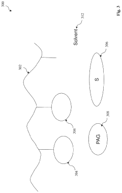
Photoacid generators (PAGs) play a crucial role in EUV resist formulations for reducing stochastic defects. Optimizing PAG concentration, distribution, and chemical structure can significantly improve pattern fidelity and reduce shot noise effects. Advanced PAGs with higher quantum efficiency and controlled diffusion characteristics help minimize line edge roughness and pattern collapse in EUV lithography processes.- PAG optimization for stochastic defect reduction in EUV resists: Photoacid generators (PAGs) play a crucial role in EUV resist formulations by generating acids upon exposure to radiation. Optimizing PAG concentration, distribution, and chemical structure can significantly reduce stochastic defects. Advanced PAGs with higher quantum efficiency and improved solubility in resist matrices help ensure uniform acid generation throughout the resist film, leading to more consistent pattern formation and fewer random defects. Strategic selection of PAGs with specific absorption characteristics matched to EUV wavelengths can enhance sensitivity while maintaining resolution.
- Quencher compounds for controlling acid diffusion and improving pattern fidelity: Quencher compounds in EUV resist formulations neutralize excess acids and control acid diffusion, which is critical for reducing stochastic defects. By carefully balancing the ratio of quenchers to PAGs, resist formulations can achieve improved line edge roughness and pattern fidelity. Advanced quencher designs with tailored basicity and diffusion properties help maintain sharp boundaries between exposed and unexposed regions. Some formulations incorporate quenchers with specific molecular structures that interact with the polymer matrix to enhance stability and reduce random variations in the development process.
- Polymer design and additives for enhanced EUV sensitivity: Advanced polymer designs and specialized additives can significantly enhance EUV resist sensitivity while reducing stochastic defects. Metal-containing additives increase EUV absorption efficiency, while carefully selected polymer structures provide improved dissolution contrast. Incorporating specific functional groups into the polymer backbone can enhance acid-catalyzed deprotection reactions and improve development characteristics. Some formulations include nanoparticles or molecular additives that modify the optical properties of the resist to optimize absorption at EUV wavelengths, resulting in more uniform exposure patterns with fewer random defects.
- Multi-trigger resist mechanisms for stochastic defect mitigation: Multi-trigger resist mechanisms require multiple chemical events to occur before solubility switching, which helps average out random variations and reduce stochastic defects. These systems often incorporate specialized additives that work synergistically with PAGs and quenchers to create more deterministic reaction pathways. By requiring multiple photons or chemical reactions to initiate the solubility change, these formulations are less susceptible to shot noise effects that contribute to stochastic defects. Some approaches include chemical amplification systems with secondary reaction pathways that help compensate for local variations in acid concentration.
- Process optimization and computational modeling for defect reduction: Process optimization techniques and computational modeling approaches help identify optimal resist formulations and processing conditions to minimize stochastic defects. Advanced simulation tools can predict the behavior of complex resist systems, allowing for rapid screening of potential formulations before experimental testing. Machine learning algorithms analyze patterns in defect formation to guide the development of improved resist compositions. Post-exposure processing techniques, such as controlled baking protocols and specialized development processes, can further reduce the impact of random variations in the resist chemistry, leading to more consistent pattern formation with fewer stochastic defects.
02 Quencher compounds for controlling acid diffusion and improving resolution
Quencher compounds in EUV resist formulations help control acid diffusion during the post-exposure bake process, thereby reducing stochastic defects. These compounds neutralize excess acids generated during exposure, improving contrast and resolution. By optimizing the quencher concentration and distribution within the resist, pattern uniformity can be enhanced and line width roughness can be minimized, leading to better overall lithographic performance.Expand Specific Solutions03 Additives for enhancing sensitivity and reducing pattern collapse
Various additives can be incorporated into EUV resist formulations to enhance sensitivity and reduce pattern collapse, which are common causes of stochastic defects. These additives include surfactants, dissolution inhibitors, and plasticizers that improve adhesion, modify surface tension, and enhance mechanical properties of the resist film. By carefully selecting and optimizing these additives, the overall performance of EUV resists can be significantly improved.Expand Specific Solutions04 Metal-containing materials for improved EUV absorption
Metal-containing materials can be incorporated into EUV resist formulations to improve EUV absorption efficiency, thereby reducing stochastic defects. These materials, including metal oxides, metal complexes, and organometallic compounds, enhance the sensitivity of the resist to EUV radiation. By increasing the absorption cross-section, these additives help to reduce the required exposure dose, minimizing shot noise and improving pattern fidelity.Expand Specific Solutions05 Multi-component resist systems for defect mitigation
Multi-component resist systems offer advanced approaches to mitigate stochastic defects in EUV lithography. These systems may include multiple PAGs with different activation wavelengths, combinations of various quenchers, or layer-structured resists. By optimizing the interaction between different components, these systems can achieve better sensitivity, resolution, and line edge roughness performance, ultimately reducing the occurrence of stochastic defects in high-resolution patterns.Expand Specific Solutions
Leading Companies in EUV Resist Development
The EUV resist defect reduction technology landscape is currently in a transitional phase, moving from early adoption to mainstream implementation as EUV lithography becomes critical for advanced semiconductor manufacturing. The market is projected to grow significantly as chipmakers advance to 5nm nodes and beyond, with an estimated value exceeding $500 million by 2025. Leading chemical suppliers including JSR, TOK, Shin-Etsu Chemical, and Sumitomo Chemical dominate the space with mature PAG and quencher technologies, while semiconductor giants like Samsung, TSMC, and IBM drive innovation through collaborative research. Academic institutions such as MIT and research labs are exploring novel additives and stochastic modeling approaches to address fundamental EUV challenges, indicating the technology remains in active development despite commercial deployment.
International Business Machines Corp.
Technical Solution: IBM has pioneered a hybrid approach to stochastic defect reduction in EUV resists through their advanced materials research program. Their technology combines traditional chemically amplified resist components with novel non-chemically amplified elements to create a balanced system that addresses fundamental stochastic challenges. IBM's approach features specially engineered PAGs with controlled solubility and diffusion characteristics, designed to maintain uniform distribution throughout the resist film. Their innovation includes the development of "smart quenchers" that selectively neutralize acids at pattern boundaries while preserving acid concentration in exposed areas, significantly reducing line edge roughness. IBM has also introduced metal-oxide nanoparticle additives that enhance EUV absorption efficiency by up to 30%, allowing for reduced exposure doses while maintaining pattern fidelity. Their multi-trigger activation mechanism requires multiple photon absorptions within proximity to generate an acid, effectively filtering out random absorption events that lead to stochastic defects.
Strengths: Exceptional pattern fidelity at extreme dimensions, reduced sensitivity to dose variations, and compatibility with existing lithography equipment. Weaknesses: Complex formulation requiring precise manufacturing controls and potentially higher material costs compared to conventional resists.
TOKYO OHKA KOGYO CO., LTD.
Technical Solution: Tokyo Ohka Kogyo (TOK) has developed a comprehensive stochastic defect reduction approach for EUV resists centered on their proprietary metal-containing resist platform. Their technology incorporates specially designed PAGs with optimized ionization efficiency and controlled diffusion characteristics to minimize shot noise effects. TOK's solution features gradient-distributed quencher molecules that create a concentration differential between pattern centers and edges, effectively suppressing pattern collapse and bridging defects. A key innovation is their multi-layer resist system that combines an EUV-sensitive top layer with a transfer layer, allowing for improved critical dimension uniformity while maintaining high sensitivity. TOK has also introduced novel polymer matrix designs with controlled polarity transitions during development, which has demonstrated up to 40% reduction in stochastic defects while maintaining sub-7nm resolution capabilities.
Strengths: Excellent balance between sensitivity and resolution, superior line edge roughness control, and compatibility with high-volume manufacturing. Weaknesses: Complex multi-component formulation requiring precise quality control and potential for increased material costs due to specialized additives.
Key Innovations in Stochastic Defect Reduction
Extreme Ultraviolet Photoresist and Method
PatentActiveUS20190384172A1
Innovation
- A photoresist composition including a polymer, a sensitizer sensitive to EUV radiation, and a photoacid generator (PAG) with a specific chemical structure where the PAG has phenyl rings bonded to sulfur, enhancing the absorption of secondary electrons and acid generation, thereby increasing the sensitivity and efficiency of the resist material.
EUV metallic resist performance enhancement via additives
PatentPendingUS20240377735A1
Innovation
- Incorporating additives such as high boiling point solvents, photo acid generators, photo base generators, quenchers, photo decomposed bases, thermal acid generators, and photo sensitivity cross-linkers into the metallic photoresist materials to enhance their shelf life and CD control, specifically targeting the instability and variability issues in metallic resists.
Material Supply Chain Analysis for EUV Resists
The supply chain for Extreme Ultraviolet (EUV) resist materials represents a critical component in semiconductor manufacturing advancement. The specialized nature of these materials, particularly those addressing stochastic defects through Photo-Acid Generators (PAGs), quenchers, and additives, has created a complex and concentrated supply ecosystem dominated by a few key players.
Japanese chemical companies maintain significant market dominance, with JSR Corporation, Tokyo Ohka Kogyo (TOK), and Shin-Etsu Chemical controlling approximately 75% of the global EUV resist market. These companies have established robust intellectual property portfolios and manufacturing expertise specifically for PAGs and quencher compounds essential to stochastic defect reduction.
European suppliers, notably BASF and Merck KGaA, have emerged as important secondary sources, focusing on specialized additives that enhance EUV resist performance. Their contributions primarily address pattern collapse prevention and sensitivity enhancement, complementing rather than directly competing with Japanese market leaders.
North American participation remains limited but strategically important, with Dow Chemical and DuPont developing novel polymer platforms and specialized quencher molecules. These companies leverage their broader chemical expertise to address specific EUV challenges, though they lack the comprehensive resist portfolios of Asian competitors.
Raw material constraints present significant supply chain vulnerabilities. Fluorinated compounds essential for advanced PAGs face increasing regulatory scrutiny due to environmental concerns, potentially limiting future availability. Similarly, rare metal compounds used in certain high-performance additives experience periodic supply constraints due to geopolitical factors affecting mining operations.
Manufacturing capacity represents another critical bottleneck, with specialized production facilities requiring cleanroom environments exceeding semiconductor fab standards in certain parameters. The limited number of facilities capable of producing ultra-pure EUV resist components creates potential single points of failure in the global supply chain.
Quality control challenges further complicate the supply landscape. The extreme sensitivity of EUV processes to even sub-parts-per-billion contaminants necessitates unprecedented purity standards, requiring specialized analytical capabilities that few suppliers can maintain consistently. This creates additional barriers to entry for potential new market participants.
Recent pandemic-related disruptions have highlighted the fragility of this specialized supply chain, prompting major semiconductor manufacturers to pursue strategic partnerships and long-term agreements with key suppliers to ensure material availability for critical production processes.
Environmental Impact of Advanced Resist Materials
The environmental impact of advanced resist materials used in EUV lithography represents a critical consideration as semiconductor manufacturing continues to evolve. Photo-acid generators (PAGs), quenchers, and additives in EUV resists contain complex chemical compounds that pose potential environmental hazards throughout their lifecycle.
The manufacturing process of these specialized materials involves energy-intensive synthesis routes and often requires hazardous precursors. Metal-based PAGs containing antimony or other heavy metals present particular concerns due to their persistence in the environment and potential toxicity. Even metal-free organic PAGs may contain fluorinated compounds that contribute to persistent organic pollutants when improperly disposed.
During semiconductor fabrication, resist materials generate waste streams that require specialized treatment. The development process typically uses TMAH (tetramethylammonium hydroxide) developers that must be neutralized before disposal. Residual resist materials removed during stripping processes create additional waste streams containing complex organic compounds and potentially toxic metals.
Volatilization of resist components during high-temperature processing steps represents another environmental concern. These emissions may contribute to air pollution if not properly captured and treated by advanced abatement systems. The semiconductor industry has made significant progress in implementing closed-loop systems to minimize these emissions, but challenges remain as resist formulations become increasingly complex.
End-of-life considerations for semiconductor devices containing residual resist materials present long-term environmental challenges. While quantities per device are minimal, the massive scale of semiconductor production means substantial cumulative impact. Proper electronic waste management becomes essential to prevent these materials from entering landfills or being processed in facilities lacking appropriate containment technologies.
The industry has responded with several sustainability initiatives. Green chemistry approaches are being explored to develop biodegradable resist components and metal-free PAG alternatives. Advanced recycling technologies aim to recover valuable components from waste resist materials. Additionally, semiconductor manufacturers are increasingly adopting life cycle assessment methodologies to quantify and minimize the environmental footprint of their resist materials.
Regulatory frameworks worldwide are evolving to address these concerns, with particular focus on PFAS (per- and polyfluoroalkyl substances) restrictions that may impact certain resist formulations. The industry must balance environmental considerations with the technical requirements for stochastic defect reduction in EUV lithography, creating opportunities for innovation in environmentally responsible resist design.
Unlock deeper insights with Patsnap Eureka Quick Research — get a full tech report to explore trends and direct your research. Try now!
Generate Your Research Report Instantly with AI Agent
Supercharge your innovation with Patsnap Eureka AI Agent Platform!