EUV Resist Metrology: SEM, AFM, And Stochastic CD Analysis
AUG 22, 20259 MIN READ
Generate Your Research Report Instantly with AI Agent
Patsnap Eureka helps you evaluate technical feasibility & market potential.
EUV Resist Metrology Evolution and Objectives
Extreme Ultraviolet (EUV) lithography represents a revolutionary advancement in semiconductor manufacturing, enabling the production of increasingly smaller and more complex integrated circuits. The evolution of EUV resist metrology has been closely tied to the development of EUV lithography itself, which began gaining significant attention in the early 2000s as traditional optical lithography approached its physical limits.
Initially, EUV resist metrology relied heavily on adapted tools from previous technology nodes, with limited resolution and precision. The early measurement techniques struggled to accurately characterize the high-aspect-ratio features and complex patterns that EUV lithography could produce. This limitation became increasingly problematic as semiconductor manufacturers pushed toward the 7nm node and beyond.
A significant turning point occurred around 2015-2017 when dedicated EUV resist metrology tools began to emerge, specifically designed to address the unique challenges of EUV lithography. These tools incorporated advanced scanning electron microscopy (SEM) capabilities with enhanced resolution and specialized algorithms for pattern recognition and measurement.
The introduction of atomic force microscopy (AFM) techniques to EUV resist metrology marked another crucial development phase. AFM provided three-dimensional topographical information that complemented the two-dimensional data from SEM, allowing for more comprehensive characterization of resist profiles and sidewall angles.
Perhaps the most transformative advancement in recent years has been the recognition and quantification of stochastic effects in EUV lithography. As feature sizes approached atomic scales, random variations in photon absorption, acid generation, and diffusion became significant factors affecting pattern fidelity and yield. This led to the development of stochastic critical dimension (CD) analysis methodologies around 2018-2020.
The primary objective of modern EUV resist metrology is to provide accurate, repeatable measurements of increasingly smaller features while accounting for stochastic variations. This includes characterizing line edge roughness (LER), line width roughness (LWR), and local critical dimension uniformity (LCDU) at the nanometer and sub-nanometer scales.
Looking forward, the field aims to develop real-time, in-line metrology capabilities that can be integrated directly into the manufacturing process, enabling immediate feedback and process adjustments. Additionally, there is a growing focus on correlating metrology data with final device performance, moving beyond simple dimensional measurements to predict functional outcomes.
Another key objective is the development of machine learning and artificial intelligence algorithms that can process the vast amounts of metrology data generated during production, identifying patterns and predicting defects before they impact yield. This represents a shift from reactive to predictive metrology approaches in the EUV lithography ecosystem.
Market Demand for Advanced Semiconductor Metrology
The semiconductor industry's relentless pursuit of Moore's Law has driven demand for increasingly sophisticated metrology solutions. As EUV lithography enables sub-7nm nodes, the market for advanced metrology tools has experienced substantial growth. Current market assessments indicate the global semiconductor metrology and inspection equipment market reached approximately $7.3 billion in 2022, with projections suggesting a compound annual growth rate of 7.8% through 2028.
EUV resist metrology specifically represents a critical and rapidly expanding segment within this market. The transition to EUV lithography has fundamentally changed measurement requirements, as feature dimensions approach atomic scales where stochastic effects become dominant factors in manufacturing yield. This has created urgent demand for metrology solutions capable of characterizing and controlling these effects.
Leading semiconductor manufacturers, including TSMC, Samsung, and Intel, have significantly increased their capital expenditure on advanced metrology equipment. TSMC alone allocated over $30 billion for capital expenditures in 2022, with a substantial portion directed toward metrology and inspection tools necessary for their 5nm and 3nm production nodes.
The market demand is primarily driven by several factors. First, yield management has become increasingly challenging at advanced nodes, with defect detection and characterization requiring unprecedented precision. A single nanometer variation in critical dimensions can result in device failure, making high-precision SEM, AFM, and stochastic analysis tools essential rather than optional.
Second, the economics of semiconductor manufacturing has shifted dramatically. The cost of yield loss at advanced nodes has escalated exponentially, with a single wafer at 3nm potentially representing hundreds of thousands of dollars in value. This economic reality has justified substantial investments in metrology solutions that can prevent such losses.
Third, the complexity of multi-patterning techniques and 3D structures in advanced semiconductor devices has created demand for metrology tools capable of measuring not just lateral dimensions but also vertical profiles and material interfaces with atomic precision.
Market analysis reveals that while traditional optical metrology continues to dominate in terms of overall market share, specialized techniques for EUV resist characterization—particularly advanced SEM with sub-nanometer resolution and AFM for surface roughness analysis—are experiencing the highest growth rates. The market segment for stochastic variation analysis tools specifically has grown by over 25% annually since 2020.
Geographically, East Asia dominates demand, accounting for approximately 65% of the global market, followed by North America at 20% and Europe at 12%. This distribution closely follows the concentration of advanced semiconductor manufacturing facilities.
Current Challenges in EUV Resist Measurement
Despite significant advancements in Extreme Ultraviolet (EUV) lithography technology, the metrology of EUV resists presents formidable challenges that impede further progress in semiconductor manufacturing. The primary difficulty lies in accurately measuring and characterizing features at sub-10nm dimensions, where traditional metrology techniques approach their fundamental limits. Scanning Electron Microscopy (SEM), while widely used, struggles with beam damage to sensitive EUV resists and exhibits limited resolution when measuring the smallest features critical to modern chip designs.
Atomic Force Microscopy (AFM) offers superior vertical resolution but faces significant throughput limitations and tip convolution effects that compromise measurement accuracy for high-aspect-ratio structures. This creates a fundamental trade-off between measurement precision and production efficiency that manufacturers must constantly navigate.
Stochastic effects in EUV resist processes represent perhaps the most significant metrology challenge. As feature sizes approach molecular dimensions of the resist materials, random variations in photon absorption, acid diffusion, and molecular aggregation create inherent pattern variability. Conventional metrology tools struggle to differentiate between measurement uncertainty and actual stochastic variations in the resist patterns, complicating process control efforts.
Line edge roughness (LER) and line width roughness (LWR) measurements have become increasingly critical quality metrics, yet current metrology solutions lack the combination of resolution, accuracy, and throughput needed for high-volume manufacturing environments. The industry faces a significant gap between what can be measured in research settings versus what is practical in production environments.
Cross-sectional analysis techniques, essential for understanding resist profiles, remain destructive and time-consuming. This limits their application in real-time process monitoring and control, forcing manufacturers to rely on indirect measurements that may not fully capture critical resist characteristics.
Data integration across multiple metrology techniques presents another significant challenge. Different tools provide complementary information, but correlating and integrating these diverse datasets requires sophisticated algorithms and reference standards that are still evolving. The lack of standardized metrology approaches for EUV resists further complicates cross-industry comparisons and technology development.
Finally, the economic challenges cannot be overlooked. Advanced metrology solutions for EUV resists require substantial capital investment, specialized expertise, and significant development time. The cost-benefit analysis for implementing cutting-edge metrology capabilities must be carefully weighed against production requirements and competitive pressures in the semiconductor industry.
Current SEM and AFM Metrology Solutions
01 SEM-based metrology for EUV resist critical dimension measurement
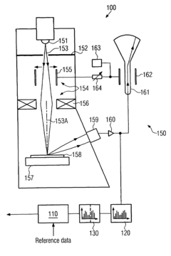
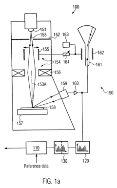
Scanning Electron Microscopy (SEM) techniques are used for measuring critical dimensions in EUV resist patterns. These methods provide high-resolution imaging of resist features, allowing for precise measurement of linewidths, spaces, and other critical dimensions. Advanced SEM techniques can detect subtle variations in resist profiles and edge roughness, which are crucial for EUV lithography where dimensions approach atomic scales. The measurements help in characterizing resist performance and optimizing lithographic processes.- SEM-based metrology for EUV resist critical dimension measurement: Scanning Electron Microscopy (SEM) techniques are widely used for measuring critical dimensions in EUV resist patterns. These methods provide high-resolution imaging of resist structures, allowing for precise measurement of feature sizes, line widths, and edge roughness. Advanced SEM techniques can detect nanometer-scale variations in resist patterns, which is crucial for EUV lithography where dimensions are extremely small. SEM-based metrology enables accurate assessment of pattern fidelity and helps in optimizing EUV resist formulations.
- AFM techniques for EUV resist characterization: Atomic Force Microscopy (AFM) provides three-dimensional topographical information of EUV resist patterns with nanometer-scale resolution. AFM techniques are particularly valuable for measuring surface roughness, line edge roughness, and line width roughness in EUV resist patterns. By scanning the surface with a mechanical probe, AFM can detect subtle variations in resist profiles that might not be visible with other techniques. This method allows for detailed analysis of resist sidewall angles and pattern collapse issues that are critical for EUV lithography performance.
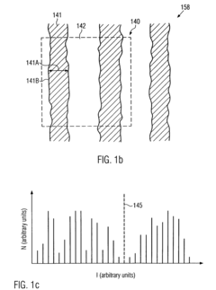
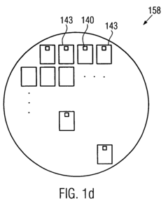
- Stochastic effects analysis in EUV resist patterns: Stochastic effects in EUV resist patterns, such as random variations in line edge roughness and critical dimension uniformity, are analyzed using specialized metrology techniques. These methods quantify the statistical distribution of pattern features to understand the fundamental limits of EUV lithography resolution. Stochastic analysis helps identify sources of variability in resist performance, including photon shot noise, acid diffusion randomness, and molecular inhomogeneities. By characterizing these stochastic effects, researchers can develop improved resist formulations with better line edge roughness and critical dimension control.
- Integrated metrology systems for EUV resist characterization: Integrated metrology systems combine multiple measurement techniques to provide comprehensive characterization of EUV resist patterns. These systems may incorporate SEM, AFM, optical scatterometry, and other methods to simultaneously evaluate different aspects of resist performance. Integrated approaches enable correlation between different measurement techniques, providing more reliable data for process control. Such systems often include automated pattern recognition and analysis software to enhance measurement throughput and consistency, which is essential for high-volume manufacturing using EUV lithography.
- Machine learning and computational methods for EUV resist metrology: Advanced computational methods and machine learning algorithms are increasingly applied to EUV resist metrology to enhance measurement accuracy and extract more information from metrology data. These approaches can identify subtle patterns in measurement data that might not be apparent through conventional analysis. Machine learning techniques help in predicting resist performance based on metrology measurements and can compensate for systematic errors in measurement tools. Computational methods also enable simulation of expected measurement results, which can be compared with actual measurements to validate resist models and improve process control.
02 AFM techniques for EUV resist surface characterization
Atomic Force Microscopy (AFM) provides three-dimensional topographical imaging of EUV resist surfaces with nanometer-scale resolution. This technique allows for detailed analysis of resist roughness, line edge roughness (LER), and line width roughness (LWR), which are critical parameters affecting device performance in advanced semiconductor manufacturing. AFM measurements can detect subtle variations in resist profiles that might not be visible with other techniques, providing valuable data for resist formulation and process optimization.Expand Specific Solutions03 Stochastic analysis methods for EUV resist pattern variability
Stochastic analysis techniques are employed to characterize random variations in EUV resist patterns caused by quantum effects and molecular interactions at extremely small dimensions. These methods use statistical approaches to quantify pattern variability, defect probability, and feature placement errors. By analyzing the stochastic behavior of resist materials, researchers can develop more robust resist formulations and process conditions that minimize random variations, improving yield and device performance in advanced semiconductor manufacturing.Expand Specific Solutions04 Integrated metrology systems for comprehensive EUV resist evaluation
Integrated metrology systems combine multiple measurement techniques such as SEM, AFM, and optical methods to provide comprehensive characterization of EUV resist patterns. These systems enable correlation between different measurement methods, offering more complete understanding of resist performance. Integrated approaches allow for in-line monitoring during semiconductor manufacturing, providing rapid feedback for process control and optimization. Such systems help identify and address various aspects of resist behavior including critical dimension uniformity, line edge roughness, and defectivity.Expand Specific Solutions05 Machine learning and computational methods for EUV resist metrology
Advanced computational techniques and machine learning algorithms are being applied to EUV resist metrology to enhance measurement accuracy and extract more information from metrology data. These methods can identify patterns in complex metrology datasets, predict resist performance, and optimize process parameters. Machine learning approaches help in addressing the challenges of measuring increasingly small features and complex patterns in EUV lithography. Computational methods also enable virtual metrology and simulation of resist behavior, reducing the need for physical measurements and accelerating development cycles.Expand Specific Solutions
Key Industry Players in Metrology Equipment
EUV Resist Metrology is currently in a growth phase, with the market expanding as semiconductor manufacturers adopt EUV lithography for advanced nodes. The global market size is projected to reach significant value due to increasing demand for smaller, more powerful chips. Technologically, the field is maturing rapidly with companies like ASML, Intel, TSMC, and Samsung leading development. Applied Materials, Tokyo Electron, and Hitachi High-Tech are advancing metrology tools including SEM and AFM for stochastic CD analysis. Research institutions like IMEC and Industrial Technology Research Institute collaborate with industry leaders to address challenges in resist performance measurement. The competitive landscape features established semiconductor equipment manufacturers alongside specialized metrology solution providers working to improve accuracy and throughput for next-generation semiconductor manufacturing.
Taiwan Semiconductor Manufacturing Co., Ltd.
Technical Solution: TSMC has developed a comprehensive EUV resist metrology framework that combines multiple measurement techniques to characterize and control stochastic effects in their advanced manufacturing processes. Their approach integrates high-resolution CD-SEM with specialized beam conditions optimized for EUV resists, alongside AFM measurements for 3D profile analysis[7]. TSMC's metrology solution features proprietary image processing algorithms that can detect and quantify sub-nanometer variations in resist patterns, enabling statistical analysis of stochastic effects across full wafers. They have implemented an automated metrology workflow that correlates SEM and AFM data with electrical test results to identify critical stochastic defects that impact device performance. Their system incorporates machine learning models trained on vast production datasets to predict yield impacts from measured stochastic variations, enabling proactive process adjustments[8]. TSMC has also developed novel sampling methodologies that optimize measurement locations across wafers to efficiently capture stochastic variations with statistical significance while maintaining production throughput.
Strengths: TSMC's metrology approach benefits from direct integration with actual high-volume manufacturing processes, providing practical insights tied to yield and device performance. Their extensive data collection enables robust statistical analysis of stochastic effects. Weaknesses: Their solutions are primarily developed for internal use rather than commercial availability, limiting broader industry access to their methodological advances.
ASML Netherlands BV
Technical Solution: ASML's EUV resist metrology solution integrates advanced SEM and AFM technologies with proprietary algorithms for stochastic CD analysis. Their YieldStar optical metrology system has been enhanced specifically for EUV resist characterization, offering sub-nanometer precision measurements. The system employs machine learning algorithms to identify and analyze stochastic defects in EUV resists, providing real-time feedback for process optimization[1]. ASML has developed a unique approach combining scatterometry with SEM imaging that allows for both surface and subsurface analysis of resist structures, critical for understanding EUV-specific effects like pattern collapse and line edge roughness. Their metrology tools feature specialized electron beam configurations that minimize damage to sensitive EUV resist materials while maintaining measurement accuracy[2]. Recent advancements include integration with their computational lithography platform for predictive modeling of stochastic variations in resist performance.
Strengths: Seamless integration with ASML's EUV lithography systems provides a comprehensive ecosystem advantage. Their metrology solutions benefit from direct knowledge of exposure conditions, enabling more accurate measurements and analysis. Weaknesses: The specialized nature of their solutions can create vendor lock-in, and the high cost of implementation may be prohibitive for smaller manufacturers.
Critical Patents in Stochastic CD Analysis
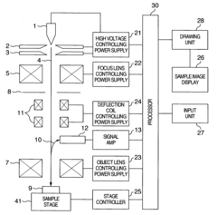
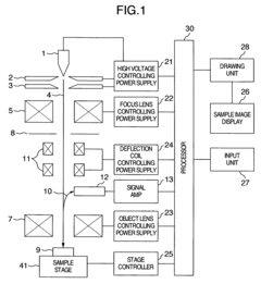
Method for controlling charged particle beam, and charged particle beam apparatus
PatentInactiveUS20050253067A1
Innovation
- A method and apparatus that control the focus, brightness, and contrast of a charged particle beam by creating an image of a first pattern, storing the control parameters, and applying them to a second pattern, reducing electron beam irradiation and minimizing sample damage.
Technique for CD measurement on the basis of area fraction determination
PatentInactiveUS7335880B2
Innovation
- A technique that uses area fractions determined from image parameters and predefined thresholds, rather than edge-based distance measurements, to estimate critical dimensions, employing higher electron beam energies to reduce image artifacts and enhance resolution, thereby improving measurement accuracy and statistical significance.
Integration with AI for Enhanced Metrology
The integration of artificial intelligence with EUV resist metrology represents a transformative approach to addressing the increasing complexity and precision demands in semiconductor manufacturing. Machine learning algorithms are now being deployed to enhance the capabilities of traditional metrology tools such as SEM, AFM, and CD-SEM, enabling more accurate and efficient stochastic defect analysis.
Deep learning models have demonstrated remarkable success in pattern recognition and image classification tasks, making them particularly suitable for analyzing the vast amounts of imaging data generated during EUV resist inspection. Convolutional neural networks (CNNs) can be trained to identify subtle variations in resist patterns that might indicate potential defects or process variations, often detecting anomalies that would be challenging for human operators or conventional algorithms to identify.
AI-powered metrology systems are increasingly capable of real-time analysis, allowing for immediate feedback during manufacturing processes. This capability significantly reduces the time between detection and correction of issues, improving overall yield and reducing costly rework. Furthermore, these systems can continuously learn from new data, becoming more accurate and efficient over time through reinforcement learning techniques.
Predictive analytics represents another promising application of AI in EUV resist metrology. By analyzing historical metrology data alongside process parameters, AI algorithms can predict potential defect formations before they occur, enabling preemptive adjustments to manufacturing processes. This predictive capability is particularly valuable for managing the stochastic effects inherent in EUV lithography.
The integration of multiple data sources through AI frameworks allows for more comprehensive metrology solutions. By combining data from SEM, AFM, and optical inspection tools, machine learning algorithms can provide a more complete picture of resist performance and potential failure modes. This multi-modal approach helps overcome the limitations of any single metrology technique.
Edge computing architectures are being developed to support AI-enhanced metrology, allowing for data processing closer to the point of collection. This approach reduces latency and bandwidth requirements while enabling more responsive control systems. The combination of edge computing with cloud-based deep learning models creates a flexible infrastructure capable of handling the computational demands of advanced metrology.
Despite these advancements, challenges remain in the widespread adoption of AI for EUV resist metrology. These include the need for extensive training datasets, concerns about algorithmic transparency, and integration with existing fab infrastructure. However, the potential benefits in terms of improved accuracy, efficiency, and yield make this an area of intense research and development activity across the semiconductor industry.
Metrology Standards and Calibration Methods
In the rapidly evolving field of EUV lithography, establishing robust metrology standards and calibration methods is crucial for ensuring measurement accuracy and consistency across different tools and facilities. The semiconductor industry has developed several standardized approaches for EUV resist metrology that address the unique challenges posed by stochastic effects and nanoscale dimensions.
The International Technology Roadmap for Semiconductors (ITRS) has established specific metrology requirements for EUV lithography, including CD uniformity targets below 1nm and line edge roughness (LER) specifications under 2nm. These standards serve as benchmarks for evaluating the performance of metrology tools and resist materials in production environments.
For SEM-based metrology, calibration artifacts with certified dimensions traceable to national metrology institutes like NIST (USA) or PTB (Germany) are widely employed. These artifacts typically consist of silicon or quartz substrates with precisely defined features that enable tool calibration across multiple magnification ranges. The calibration process must account for electron beam interactions with EUV resists, which can cause shrinkage and measurement bias.
AFM calibration for EUV resist metrology follows similar principles but requires additional considerations for tip characterization. Standard reference materials with known step heights and pitch values are used to calibrate the vertical and lateral response of AFM systems. Blind reconstruction algorithms have been developed to deconvolve tip-sample interactions, improving measurement accuracy for high-aspect-ratio resist features.
Stochastic CD analysis presents unique standardization challenges due to its statistical nature. The industry has adopted standardized sampling protocols that specify minimum feature counts (typically >1000 features) required for statistically significant analysis. Standard metrics include CD uniformity (CDU), line width roughness (LWR), and line edge roughness (LER), with clearly defined measurement and filtering algorithms to ensure consistency.
Cross-platform calibration methods have become increasingly important as labs employ multiple metrology techniques. Reference samples measured by transmission electron microscopy (TEM) often serve as "golden standards" for calibrating both SEM and AFM measurements. Round-robin testing programs, where identical samples are measured at different facilities, help establish measurement uncertainty budgets and identify systematic biases between tools.
The metrology community has also developed standardized data formats and analysis protocols for EUV resist characterization. These include specifications for power spectral density (PSD) analysis of roughness data and statistical methods for quantifying stochastic variations, ensuring that results can be meaningfully compared across research groups and manufacturing sites.
Unlock deeper insights with Patsnap Eureka Quick Research — get a full tech report to explore trends and direct your research. Try now!
Generate Your Research Report Instantly with AI Agent
Supercharge your innovation with Patsnap Eureka AI Agent Platform!