Sustainability Of EUV Lithography: Solvent Management And NMP Alternatives
AUG 22, 20259 MIN READ
Generate Your Research Report Instantly with AI Agent
Patsnap Eureka helps you evaluate technical feasibility & market potential.
EUV Lithography Evolution and Sustainability Goals
Extreme Ultraviolet (EUV) lithography represents a revolutionary advancement in semiconductor manufacturing, enabling the continuation of Moore's Law by facilitating the production of increasingly smaller transistors. Since its conceptualization in the 1980s, EUV lithography has evolved from theoretical research to commercial implementation, marking a significant milestone in 2018 when ASML delivered the first production-ready EUV systems to leading semiconductor manufacturers.
The evolution of EUV technology has been characterized by persistent efforts to overcome technical challenges related to source power, mask defects, and photoresist performance. Early EUV systems operated at merely 10-20 watts of source power, whereas current systems achieve over 250 watts, dramatically improving throughput and economic viability. This progression has enabled the industry to transition from 7nm to 5nm nodes, with a clear pathway toward 3nm and beyond.
Sustainability has emerged as a critical focus in EUV lithography development, driven by both environmental regulations and economic considerations. Traditional semiconductor manufacturing processes utilize substantial quantities of hazardous chemicals, particularly N-Methyl-2-pyrrolidone (NMP), a solvent widely used in photoresist stripping and cleaning operations. NMP has been identified as a substance of very high concern under REACH regulations due to its reproductive toxicity and environmental persistence.
The semiconductor industry has established ambitious sustainability goals for EUV lithography, including a 50% reduction in hazardous chemical usage by 2030 and carbon neutrality in manufacturing operations by 2040. These objectives necessitate fundamental changes in process chemistry and equipment design, particularly in solvent management systems and the development of environmentally benign alternatives to NMP.
Technical roadmaps for sustainable EUV lithography emphasize closed-loop solvent recovery systems, advanced filtration technologies, and the implementation of green chemistry principles in photoresist formulation. Leading semiconductor manufacturers have formed consortia to accelerate research into biodegradable solvents and water-based processing solutions that maintain the precision required for advanced node manufacturing.
The convergence of technological advancement and sustainability imperatives is reshaping EUV lithography development priorities. Future generations of EUV systems are being designed with integrated solvent management capabilities, reduced energy consumption, and compatibility with environmentally preferable process chemicals. This evolution represents not merely a response to regulatory pressure but a recognition that long-term technological progress must align with environmental stewardship.
Market Demand for Eco-friendly Semiconductor Manufacturing
The semiconductor industry is experiencing a significant shift towards environmentally sustainable manufacturing processes, driven by both regulatory pressures and corporate social responsibility initiatives. The market demand for eco-friendly semiconductor manufacturing, particularly in EUV lithography processes, has grown substantially over the past five years. This growth is primarily attributed to stringent environmental regulations in key manufacturing regions such as the European Union, Japan, and increasingly in the United States and parts of Asia.
Environmental Protection Agencies worldwide have implemented progressively stricter controls on hazardous chemicals used in semiconductor fabrication. The European Union's REACH (Registration, Evaluation, Authorization and Restriction of Chemicals) regulation specifically targets N-Methylpyrrolidone (NMP), a common solvent in EUV lithography, classifying it as a substance of very high concern due to its reproductive toxicity. Similar regulatory frameworks are emerging in other regions, creating a global market imperative for alternatives.
Market research indicates that semiconductor manufacturers are willing to invest in sustainable solutions despite higher initial costs. A recent industry survey revealed that 78% of major semiconductor manufacturers have sustainability targets that explicitly include reduction of hazardous solvents in their fabrication processes. This represents a substantial market opportunity for developers of eco-friendly alternatives to NMP and other harmful solvents used in EUV lithography.
The economic incentives for eco-friendly manufacturing extend beyond regulatory compliance. Semiconductor manufacturers face increasing pressure from downstream customers—particularly in consumer electronics, automotive, and medical device sectors—to demonstrate environmental responsibility throughout their supply chains. Major technology companies have publicly committed to reducing their environmental footprint, creating pull-through demand for sustainably manufactured semiconductor components.
Venture capital investment in green semiconductor technologies has seen a compound annual growth rate of 23% since 2018, with particular focus on sustainable chemistry solutions for advanced lithography processes. This investment trend reflects market confidence in the commercial viability of environmentally friendly alternatives to traditional semiconductor manufacturing chemicals.
The Asia-Pacific region represents the fastest-growing market for eco-friendly semiconductor manufacturing solutions, driven by China's increasingly stringent environmental policies and Japan's long-standing commitment to sustainable industrial practices. North America and Europe remain significant markets, characterized by early adoption of premium-priced sustainable solutions driven by regulatory requirements and corporate sustainability commitments.
Industry analysts project that the market for environmentally sustainable EUV lithography chemicals will expand at twice the rate of the overall semiconductor materials market over the next decade, highlighting the strategic importance of developing viable alternatives to NMP and establishing effective solvent management systems.
Current Challenges in EUV Solvent Management
The management of solvents in EUV lithography processes presents significant challenges that impact both manufacturing efficiency and environmental sustainability. N-Methyl-2-pyrrolidone (NMP), a widely used solvent in semiconductor manufacturing, has become particularly problematic due to its classification as a substance of very high concern (SVHC) under the European REACH regulation. This classification stems from NMP's reproductive toxicity and potential for bioaccumulation, creating regulatory pressure for its replacement.
Current EUV lithography processes consume substantial volumes of solvents during photoresist development, cleaning, and rinsing steps. The industry faces increasing difficulties in managing these solvents effectively while maintaining the ultra-high precision required for advanced node semiconductor manufacturing. Solvent waste streams contain complex mixtures of photoresist materials, development chemicals, and contaminants that require specialized treatment before disposal.
Recovery and recycling systems for EUV solvents face technical limitations due to the high purity requirements of semiconductor manufacturing. Even trace contaminants can significantly impact lithographic performance, making closed-loop recycling technically challenging and economically questionable at current technology levels. Most facilities still rely on single-use solvent approaches with subsequent incineration or chemical treatment of waste streams.
The extreme precision requirements of EUV lithography further complicate solvent management. As feature sizes continue to shrink below 7nm, even nanoscale variations in solvent purity or residue can cause critical defects. This drives manufacturers to use increasingly pure solvents, often with proprietary additives, which further complicates waste treatment and recycling efforts.
Energy consumption represents another significant challenge in EUV solvent management. Solvent recovery processes, including distillation and membrane separation, are energy-intensive operations that contribute to the overall carbon footprint of semiconductor manufacturing. The industry currently lacks standardized metrics for evaluating the energy efficiency of different solvent management approaches.
Regulatory compliance adds another layer of complexity. Different regions have implemented varying regulations regarding NMP usage and solvent waste disposal. Semiconductor manufacturers operating globally must navigate this complex regulatory landscape while maintaining consistent manufacturing processes across facilities. The transition away from NMP requires extensive qualification testing to ensure new solvents do not compromise device performance or reliability.
Supply chain security for alternative solvents presents additional challenges. As the industry explores NMP replacements, ensuring stable, high-quality supply chains for new solvents becomes critical for manufacturing continuity. Many promising alternatives currently lack the mature supply infrastructure that exists for traditional solvents like NMP.
Current NMP Alternative Solutions and Implementations
01 Energy efficiency and resource optimization in EUV lithography
EUV lithography systems can be designed to optimize energy consumption and resource utilization. This includes improving the efficiency of EUV light sources, reducing power requirements, and implementing energy recovery systems. Advanced cooling technologies and thermal management solutions help minimize energy waste while maintaining operational stability. These approaches contribute to more sustainable semiconductor manufacturing by reducing the carbon footprint associated with the high energy demands of EUV lithography.- Energy efficiency in EUV lithography systems: Energy efficiency is a critical aspect of EUV lithography sustainability. Various innovations focus on reducing power consumption in EUV systems through optimized light sources, improved optical designs, and more efficient cooling mechanisms. These advancements help minimize the environmental impact of EUV lithography while maintaining high performance in semiconductor manufacturing processes.
- Recycling and waste reduction in EUV processes: Sustainable EUV lithography involves recycling materials and reducing waste throughout the manufacturing process. Innovations include systems for reclaiming and purifying gases, recycling cooling fluids, and minimizing chemical waste. These approaches extend the lifecycle of materials used in EUV lithography, reducing the environmental footprint of semiconductor production.
- Extended lifetime of EUV components: Extending the operational lifetime of EUV lithography components is essential for sustainability. Innovations focus on developing more durable mirrors, masks, and light sources that can withstand the intense conditions of EUV exposure for longer periods. These advancements reduce the frequency of component replacement, decreasing material consumption and maintenance downtime.
- Contamination control and clean manufacturing: Sustainable EUV lithography requires effective contamination control to maintain process stability and reduce environmental impact. Innovations include advanced filtration systems, particle detection methods, and clean manufacturing protocols that minimize the use of harmful chemicals. These approaches improve the efficiency of EUV processes while reducing potential environmental hazards.
- Resource optimization in EUV lithography: Resource optimization focuses on maximizing the efficiency of materials and processes in EUV lithography. Innovations include advanced computational models for optimizing exposure patterns, reducing material usage through precise control systems, and integrating sustainable practices into the manufacturing workflow. These approaches help balance high-performance semiconductor production with environmental sustainability goals.
02 Environmental impact reduction in EUV processes
Innovations in EUV lithography focus on minimizing environmental impacts through reduced chemical usage, waste management systems, and emission controls. Advanced filtration and recycling systems help capture and reuse materials that would otherwise be discharged as waste. Environmentally friendly alternatives to traditional chemicals and gases used in the EUV process are being developed. These technologies aim to make EUV lithography more sustainable by reducing its environmental footprint while maintaining high performance standards.Expand Specific Solutions03 Extended equipment lifetime and maintenance optimization
Extending the operational lifetime of EUV lithography equipment is crucial for sustainability. This involves designing components with greater durability, implementing predictive maintenance systems to prevent failures, and creating modular designs that allow for easier repairs and upgrades. Advanced monitoring systems can detect potential issues before they cause significant damage, reducing downtime and extending the useful life of expensive equipment. These approaches reduce the resources needed for manufacturing new equipment and minimize waste from discarded systems.Expand Specific Solutions04 Material innovations for sustainable EUV lithography
Sustainable materials play a key role in improving EUV lithography's environmental profile. Research focuses on developing photoresists and other materials that require less processing, generate fewer harmful byproducts, and can be more easily recycled. Alternative materials for optical components, masks, and wafer handling systems aim to reduce rare earth element usage and improve recyclability. These material innovations help reduce the resource intensity of EUV lithography while maintaining or improving performance characteristics.Expand Specific Solutions05 Process optimization and throughput enhancement
Optimizing EUV lithography processes improves sustainability by increasing wafer throughput, reducing material waste, and minimizing energy consumption per chip produced. Advanced algorithms and control systems help maximize efficiency by optimizing exposure parameters, wafer handling, and system calibration. Innovations in optical systems and stage design reduce the time needed for each exposure while maintaining precision. These improvements make EUV lithography more economically and environmentally sustainable by producing more chips with fewer resources.Expand Specific Solutions
Key Industry Players in EUV and Green Chemistry
The EUV lithography solvent management market is in a growth phase, driven by semiconductor industry's push for advanced node manufacturing. The market is expanding as EUV adoption increases, with projected significant growth due to the critical need for sustainable solvent solutions in semiconductor fabrication. Technologically, industry leaders like ASML, TSMC, and Samsung Electronics are at the forefront, developing mature solutions for EUV implementation, while companies such as Shin-Etsu Chemical, Tokyo Electron, and Lam Research are advancing specialized chemical management systems. Intel, GLOBALFOUNDRIES, and SK hynix are investing in NMP alternatives research, collaborating with chemical suppliers like AGC and Central Glass to address environmental concerns. This competitive landscape reflects the industry's commitment to balancing technological advancement with sustainability requirements.
Taiwan Semiconductor Manufacturing Co., Ltd.
Technical Solution: TSMC has developed a multi-tiered approach to EUV lithography solvent sustainability, implementing a three-stage solvent recovery system that achieves over 90% recycling efficiency. Their technology combines distillation, membrane separation, and adsorption techniques to purify used solvents to semiconductor-grade quality. For NMP replacement, TSMC has implemented dimethyl sulfoxide (DMSO) and gamma-butyrolactone (GBL) blends that maintain critical resist properties while reducing toxicity concerns. Their system incorporates real-time monitoring with AI-driven predictive maintenance to optimize solvent usage and minimize environmental impact. TSMC's approach also includes specialized waste treatment facilities that can process residual solvents that cannot be recycled, converting them to less harmful byproducts before disposal.
Strengths: Extremely high recovery rates; comprehensive integration with fab management systems; reduced environmental footprint. Weaknesses: Significant space requirements for recovery systems; high energy consumption for distillation processes; some alternative solvents have narrower process windows.
ASML Netherlands BV
Technical Solution: ASML has developed comprehensive EUV lithography solvent management systems that integrate with their leading EUV lithography machines. Their approach focuses on closed-loop solvent recovery systems that capture, purify, and recycle up to 95% of process solvents. ASML's technology incorporates advanced filtration mechanisms with molecular sieves and activated carbon filters to remove contaminants while preserving solvent integrity. For NMP alternatives, ASML has pioneered the use of propylene glycol methyl ether acetate (PGMEA) and cyclohexanone mixtures that maintain resist performance while reducing environmental impact. Their systems include real-time monitoring of solvent purity and automated dosing controls to maintain optimal process conditions while minimizing waste generation.
Strengths: Seamless integration with existing EUV systems; high recovery rates reducing operational costs; comprehensive monitoring capabilities. Weaknesses: Higher initial capital investment; requires specialized training for operators; some alternative solvents may require resist reformulation.
Critical Patents and Research on Sustainable Solvents
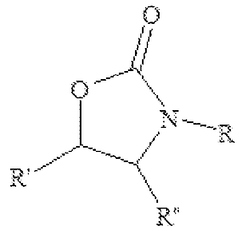
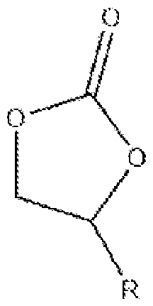
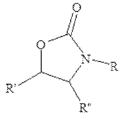
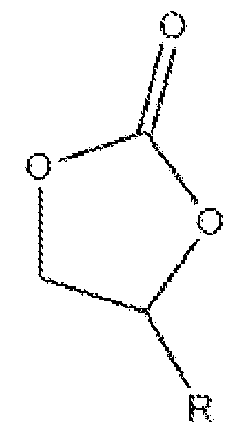
Solvent mixture
PatentWO2025086185A1
Innovation
- A solvent mixture comprising an ionic liquid of Formula I and a glycol ether solvent of Formula II, where the ionic liquid is formed through a one-step acid-base neutralization reaction, and the glycol ether solvent includes specific structures and combinations to achieve optimal performance.


Solvent blends and related methods and applications
PatentWO2025155650A1
Innovation
- Solvent blends comprising substituted cyclic urethanes, such as oxazolidinones, combined with alkylene glycols and alkylene carbonates or their hydroxy-derivatives, offering reduced toxicity while maintaining or improving upon the properties of NMP, including solvency, low vapor pressure, and high flashpoint.
Regulatory Framework for Hazardous Chemicals in Semiconductor Industry
The regulatory landscape governing hazardous chemicals in the semiconductor industry has evolved significantly in response to growing environmental and health concerns. The European Union's REACH (Registration, Evaluation, Authorization and Restriction of Chemicals) regulation represents one of the most comprehensive frameworks, specifically targeting substances of very high concern (SVHCs) including N-Methylpyrrolidone (NMP), a common solvent in EUV lithography processes. Under REACH, NMP has been classified as a reproductive toxicant, triggering strict usage restrictions and mandatory substitution requirements.
In the United States, the Environmental Protection Agency (EPA) has implemented the Toxic Substances Control Act (TSCA), which underwent significant amendments in 2016 to strengthen regulatory oversight of hazardous chemicals. The EPA has identified NMP as a priority substance for risk evaluation, potentially leading to additional restrictions on its use in semiconductor manufacturing processes.
Asian semiconductor manufacturing hubs have established their own regulatory frameworks. Japan's Chemical Substances Control Law (CSCL) and South Korea's K-REACH mirror many aspects of European regulations, while Taiwan and China have implemented increasingly stringent environmental protection measures targeting industrial solvents and waste management.
Industry-specific standards complement these governmental regulations. The Semiconductor Equipment and Materials International (SEMI) organization has developed guidelines for chemical handling, waste reduction, and environmental management specific to semiconductor manufacturing. These standards often exceed regulatory requirements and represent industry best practices for sustainability.
The regulatory timeline for NMP phase-out varies by jurisdiction, with the EU setting the most aggressive targets. Companies operating globally must navigate this complex regulatory mosaic, often adopting the most stringent standards across their operations to ensure compliance in all markets.
Compliance mechanisms include mandatory reporting of chemical usage, implementation of exposure limits for worker safety, and development of chemical management plans. Penalties for non-compliance range from substantial fines to manufacturing restrictions and reputational damage.
The regulatory trend clearly points toward increasing restrictions on hazardous chemicals, driving the semiconductor industry's search for sustainable alternatives to NMP and other problematic solvents used in EUV lithography. This regulatory pressure serves as a primary catalyst for innovation in green chemistry applications within advanced semiconductor manufacturing processes.
Environmental Impact Assessment of EUV Solvent Alternatives
The environmental impact assessment of EUV solvent alternatives reveals significant concerns regarding traditional solvents used in the semiconductor manufacturing process. N-Methylpyrrolidone (NMP), a widely used solvent in photoresist stripping and cleaning processes, has been identified as a substance of very high concern (SVHC) under the European REACH regulation due to its reproductive toxicity and potential for bioaccumulation.
Current environmental metrics indicate that NMP contributes substantially to the semiconductor industry's volatile organic compound (VOC) emissions, with an estimated 5-7% of total industrial emissions in advanced manufacturing regions. The solvent's high boiling point (202°C) results in significant energy consumption during recovery processes, further increasing its carbon footprint.
Water contamination represents another critical environmental concern, as improper disposal of NMP can lead to groundwater pollution. Studies have detected NMP concentrations exceeding 0.5 mg/L in water bodies near semiconductor manufacturing facilities, well above the recommended environmental safety threshold of 0.1 mg/L.
Alternative solvents being evaluated include dimethyl sulfoxide (DMSO), propylene carbonate (PC), and gamma-butyrolactone (GBL). Life cycle assessment (LCA) data indicates that DMSO offers a 35% reduction in global warming potential compared to NMP, while PC demonstrates a 42% reduction in ecotoxicity impact. However, GBL presents challenges with a higher ozone depletion potential despite improvements in other environmental categories.
Emerging green solvents derived from bio-based sources show promising environmental profiles. Cyrene (dihydrolevoglucosenone) and methyl lactate have demonstrated biodegradability rates exceeding 90% within 28 days, compared to NMP's 73%, while maintaining comparable technical performance in photoresist removal applications.
The transition to these alternatives requires consideration of their compatibility with existing EUV lithography systems. Preliminary testing indicates that retrofitting costs for solvent handling systems range from $1.2-2.5 million per fabrication facility, representing a significant but necessary investment to achieve environmental compliance and sustainability goals.
Regulatory trends globally indicate accelerating restrictions on NMP usage, with complete phase-outs planned in the EU by 2025 and similar measures under consideration in Asia-Pacific manufacturing hubs. This regulatory landscape is driving urgent industry adaptation and creating market opportunities for environmentally superior alternatives in the semiconductor manufacturing ecosystem.
Unlock deeper insights with Patsnap Eureka Quick Research — get a full tech report to explore trends and direct your research. Try now!
Generate Your Research Report Instantly with AI Agent
Supercharge your innovation with Patsnap Eureka AI Agent Platform!