Roadmap To Sub-10 nm Half-Pitch With High-NA EUV Materials
AUG 22, 202510 MIN READ
Generate Your Research Report Instantly with AI Agent
Patsnap Eureka helps you evaluate technical feasibility & market potential.
High-NA EUV Lithography Background and Objectives
Extreme Ultraviolet (EUV) lithography represents a revolutionary advancement in semiconductor manufacturing, enabling the continuation of Moore's Law beyond the limitations of traditional optical lithography. Since its conceptualization in the 1980s, EUV technology has evolved from theoretical research to commercial implementation, with significant milestones achieved in the past decade. The industry's relentless pursuit of smaller feature sizes has now led to the development of High Numerical Aperture (High-NA) EUV systems, representing the next frontier in lithographic technology.
High-NA EUV lithography builds upon conventional EUV systems by increasing the numerical aperture from 0.33 to 0.55, theoretically enabling resolution improvements of approximately 70%. This technological leap aims to facilitate the production of semiconductor devices with half-pitch dimensions below 10 nanometers, supporting the semiconductor industry's roadmap for the next generation of integrated circuits.
The evolution toward High-NA EUV has been driven by the fundamental physical limitations of conventional lithography techniques. As device dimensions approached the wavelength of light used in lithography, diffraction effects became increasingly problematic. The 13.5 nm wavelength of EUV light represented a significant improvement over deep ultraviolet (DUV) systems, and High-NA EUV further extends these capabilities through enhanced optical designs.
The primary objective of High-NA EUV technology is to enable mass production of semiconductor devices at the 3 nm node and beyond, maintaining the historical cadence of semiconductor scaling. This advancement is critical for supporting emerging applications in artificial intelligence, quantum computing, and advanced mobile communications that demand unprecedented computational power and energy efficiency.
Beyond resolution enhancement, High-NA EUV aims to address several key challenges in semiconductor manufacturing, including pattern fidelity, overlay accuracy, and throughput optimization. These improvements are essential for maintaining economic viability as manufacturing complexity increases with each technology node.
Material innovation represents a crucial component of the High-NA EUV roadmap. Novel resist materials must simultaneously deliver enhanced resolution, reduced line edge roughness, and improved sensitivity—a challenging combination often referred to as the "RLS triangle." Additionally, these materials must demonstrate compatibility with increasingly complex multi-patterning schemes and be environmentally sustainable.
The successful implementation of High-NA EUV technology requires unprecedented collaboration across the semiconductor ecosystem, involving equipment manufacturers, material suppliers, chip designers, and research institutions. This collaborative approach has been instrumental in overcoming the numerous technical hurdles encountered throughout EUV's development history and will remain essential as the industry pursues sub-10 nm half-pitch dimensions.
Market Demand Analysis for Sub-10 nm Semiconductor Nodes
The semiconductor industry's push towards sub-10 nm nodes is driven by relentless market demand for higher performance, lower power consumption, and increased functionality in electronic devices. This technological advancement represents a critical inflection point in semiconductor manufacturing, with significant implications for multiple high-value markets.
Consumer electronics continues to be a primary driver, with smartphones, tablets, and wearable devices requiring increasingly powerful yet energy-efficient processors. Market research indicates that the global smartphone semiconductor content value is projected to grow substantially as devices incorporate more advanced AI capabilities, enhanced imaging systems, and support for next-generation connectivity standards like 6G.
Data centers and cloud computing infrastructure represent another substantial market segment demanding sub-10 nm technology. The exponential growth in data processing requirements, accelerated by AI and machine learning workloads, necessitates chips with higher transistor densities and improved performance per watt metrics. This segment is experiencing particularly strong growth as enterprises globally accelerate their digital transformation initiatives.
Automotive electronics has emerged as a rapidly expanding market for advanced semiconductor nodes. The transition toward autonomous driving systems, electric vehicles, and connected car technologies requires sophisticated processing capabilities that can only be delivered through cutting-edge semiconductor manufacturing processes. Industry forecasts suggest that semiconductor content in premium vehicles will continue to increase dramatically over the next decade.
The artificial intelligence and machine learning sector presents perhaps the most compelling case for sub-10 nm technology adoption. Training and inference for large AI models demand unprecedented computational efficiency, driving the need for specialized processors manufactured at the most advanced nodes available.
From a geographical perspective, demand for sub-10 nm technology is concentrated in regions with strong technology ecosystems. East Asia remains the dominant manufacturing hub, while North America leads in design innovation. Europe is investing heavily to establish sovereign capabilities in advanced semiconductor manufacturing.
Supply chain considerations have become increasingly important in market demand analysis. Recent global disruptions have highlighted vulnerabilities in the semiconductor supply chain, prompting governments worldwide to invest in domestic manufacturing capabilities for advanced nodes. This geopolitical dimension has added complexity to market dynamics but also created new opportunities for diversification in the supply base.
The transition to sub-10 nm nodes represents a significant economic opportunity, with the total addressable market for devices manufactured at these advanced nodes projected to grow substantially over the next five years, despite the increasing costs and technical challenges associated with pushing the boundaries of semiconductor manufacturing technology.
Current Status and Challenges in High-NA EUV Technology
High-NA EUV lithography represents the next evolutionary step in semiconductor manufacturing technology, promising to enable feature sizes below 10 nm half-pitch. Currently, the industry has achieved mass production using conventional 0.33 NA EUV systems, capable of approximately 13 nm resolution. However, the transition to High-NA EUV (0.55 NA) faces significant technical challenges despite substantial progress in research and development.
The global landscape of High-NA EUV development shows concentration in specific regions. Europe maintains leadership through ASML's monopoly on EUV scanner production, while Japan contributes critical components such as mirrors and optical systems. The United States leads in resist materials development, and South Korea and Taiwan serve as primary implementation sites due to their semiconductor manufacturing dominance.
From a technical perspective, several critical challenges impede High-NA EUV implementation. The increased numerical aperture necessitates fundamental redesigns of optical systems, including more complex mirror arrangements and tighter tolerances. This has resulted in significantly larger and more expensive tools, with current High-NA EUV systems estimated to cost over $300 million per unit.
Resist materials present another major hurdle. Current chemically amplified resists (CARs) struggle with the resolution-sensitivity-line edge roughness trade-off at sub-10 nm dimensions. Metal-oxide resists show promise but face integration challenges with existing processes. Additionally, stochastic effects become increasingly problematic at these dimensions, causing random variations that impact yield and reliability.
Mask infrastructure represents another significant challenge. High-NA EUV requires new mask architectures to accommodate the anamorphic optical design (different magnification factors in x and y directions). This necessitates new inspection tools, defect mitigation strategies, and pellicle solutions capable of withstanding intense EUV radiation while maintaining transparency.
Power source limitations continue to constrain throughput. Current EUV sources deliver approximately 250W, but High-NA systems require significantly higher power to maintain economically viable throughput. Researchers are exploring laser-produced plasma improvements and alternative source concepts to address this bottleneck.
Integration challenges extend to metrology and inspection capabilities. Existing tools struggle to accurately measure and inspect features at sub-10 nm dimensions, creating difficulties in process control and defect identification. New metrology approaches utilizing advanced computational techniques and multi-signal analysis are under development but remain immature.
Despite these challenges, the industry continues to make progress. ASML has shipped its first High-NA EUV research tools to imec, with initial production tools expected by 2025-2026. Intel, Samsung, and TSMC have announced integration of High-NA EUV into their roadmaps for 2 nm nodes and beyond, signaling industry commitment to overcoming these technical hurdles.
Current Material Solutions for High-NA EUV Implementation
01 High-NA EUV lithography materials for improved resolution
High-NA (numerical aperture) extreme ultraviolet (EUV) lithography materials are designed to achieve smaller half-pitch dimensions, enabling the production of more advanced semiconductor devices. These materials are specifically formulated to work with high-NA EUV systems that offer improved resolution capabilities compared to conventional EUV lithography. The specialized photoresist materials are optimized for the shorter wavelengths and higher numerical apertures used in these advanced systems.- High-NA EUV lithography materials for improved resolution: High-NA (Numerical Aperture) EUV lithography materials are designed to achieve smaller half-pitch dimensions, enabling the production of more advanced semiconductor devices. These materials are specifically formulated to work with high numerical aperture EUV systems, which can focus light more precisely to create finer patterns. The specialized photoresist materials are optimized for sensitivity to EUV wavelengths while maintaining pattern fidelity at extremely small dimensions.
- Photoresist compositions for sub-10nm half-pitch patterning: Advanced photoresist compositions are developed specifically for achieving sub-10nm half-pitch resolution in EUV lithography. These formulations contain carefully selected polymers, photoacid generators, and additives that enhance sensitivity to EUV radiation while minimizing line edge roughness. The chemical amplification mechanisms in these resists are optimized to provide high contrast and resolution at extremely small feature sizes required for next-generation semiconductor manufacturing.
- Optical systems and components for High-NA EUV lithography: Specialized optical systems and components are essential for High-NA EUV lithography to achieve smaller half-pitch dimensions. These include advanced mirror designs, precision optical elements, and sophisticated illumination systems that maximize the resolution capabilities of EUV light. The optical components are engineered to minimize aberrations and maximize contrast at the wafer level, enabling the creation of extremely fine patterns required for advanced semiconductor nodes.
- Process optimization techniques for High-NA EUV patterning: Various process optimization techniques are employed to enhance the performance of High-NA EUV lithography for achieving smaller half-pitch dimensions. These include multi-patterning strategies, focus-exposure optimization, and advanced development processes. Computational lithography methods are also utilized to predict and compensate for process variations, ensuring consistent pattern formation at extremely small dimensions across the entire wafer.
- Materials for EUV mask fabrication and defect mitigation: Specialized materials are developed for EUV mask fabrication to support High-NA lithography and smaller half-pitch dimensions. These materials include advanced absorber layers, reflective multilayers, and protective pellicles that maintain pattern integrity during the lithography process. Defect mitigation strategies are incorporated into these materials to minimize the impact of mask defects on the final pattern, which becomes increasingly critical as feature sizes decrease with High-NA EUV technology.
02 Photoresist compositions for high-resolution patterning
Advanced photoresist compositions are developed specifically for high-resolution patterning in high-NA EUV lithography. These materials incorporate specialized polymers, photoacid generators, and additives that enhance sensitivity to EUV radiation while maintaining pattern fidelity at extremely small half-pitch dimensions. The chemical formulations are designed to provide high contrast, low line edge roughness, and excellent etch resistance, which are critical for achieving the smallest possible feature sizes in semiconductor manufacturing.Expand Specific Solutions03 Optical systems and components for high-NA EUV lithography
Specialized optical systems and components are essential for high-NA EUV lithography to achieve reduced half-pitch dimensions. These include advanced mirror designs, precision optical elements, and sophisticated illumination systems that maximize the resolution capabilities of EUV exposure tools. The optical components are engineered to minimize aberrations and maximize the numerical aperture, enabling the projection of extremely fine patterns onto semiconductor substrates with high accuracy and fidelity.Expand Specific Solutions04 Process optimization techniques for high-NA EUV patterning
Various process optimization techniques are employed to enhance the performance of high-NA EUV lithography for achieving smaller half-pitch dimensions. These include multi-patterning strategies, focus-exposure optimization, and advanced development processes that maximize resolution and pattern fidelity. Additional techniques such as post-exposure bake optimization, development process refinement, and etch process tuning are also critical for realizing the full resolution potential of high-NA EUV materials and systems.Expand Specific Solutions05 Metrology and inspection methods for high-NA EUV lithography
Specialized metrology and inspection methods are developed to accurately measure and characterize the extremely small features produced by high-NA EUV lithography. These methods include advanced scanning electron microscopy techniques, optical scatterometry, and atomic force microscopy adapted for sub-nanometer precision. The metrology solutions enable precise measurement of critical dimensions, overlay accuracy, and defect detection at the reduced half-pitch dimensions achievable with high-NA EUV materials and processes.Expand Specific Solutions
Key Industry Players in High-NA EUV Development
The high-NA EUV lithography market for sub-10 nm semiconductor manufacturing is in its early growth phase, with significant R&D investments driving technological advancement. Major semiconductor equipment manufacturers like ASML (through Carl Zeiss SMT) and Tokyo Electron are competing with foundry giants TSMC and SMIC to overcome critical technical challenges. Research institutions including MIT, IMEC, and Chinese Academy of Sciences are collaborating with industry leaders IBM, Lam Research, and Synopsys to develop specialized materials and processes. The ecosystem is characterized by strategic partnerships between materials suppliers (Pixelligent, FUJIFILM) and semiconductor manufacturers, with competition intensifying as companies race to commercialize high-NA EUV technology for next-generation chip production, expected to reach significant market scale by 2025-2027.
International Business Machines Corp.
Technical Solution: IBM has developed a comprehensive approach to sub-10 nm lithography using High-NA EUV technology. Their solution combines advanced photoresist materials with novel underlayer technologies to enhance pattern fidelity. IBM's research focuses on metal-oxide based resists that offer improved sensitivity and lower line edge roughness (LER) compared to traditional chemically amplified resists. They've demonstrated successful patterning of 8nm half-pitch features using their proprietary resist formulations combined with optimized exposure conditions. IBM has also pioneered the development of directed self-assembly (DSA) techniques that work synergistically with High-NA EUV to further improve resolution limits. Their integrated approach includes computational lithography methods that optimize mask designs specifically for High-NA systems, accounting for the unique imaging characteristics of these tools.
Strengths: IBM's extensive research infrastructure and deep expertise in semiconductor manufacturing enables comprehensive materials development. Their integrated approach combining resist chemistry, underlayer technology, and computational methods provides a holistic solution. Weaknesses: Implementation costs are extremely high, and the technology requires significant infrastructure investment to deploy in production environments.
Taiwan Semiconductor Manufacturing Co., Ltd.
Technical Solution: TSMC has developed a multi-faceted approach to sub-10nm half-pitch lithography using High-NA EUV technology. Their solution integrates advanced inorganic resist materials with sophisticated process control techniques. TSMC's proprietary metal-oxide resist formulations demonstrate sensitivity below 20 mJ/cm² while maintaining line edge roughness under 2nm, critical for sub-10nm patterning. Their approach incorporates specialized underlayer materials that enhance adhesion and reduce pattern collapse at extreme dimensions. TSMC has also pioneered advanced etch transfer techniques specifically optimized for High-NA EUV patterned features, ensuring pattern fidelity through the manufacturing process. Their comprehensive solution includes customized computational lithography tools that account for the unique optical properties of High-NA systems, including polarization effects and mask 3D effects that become critical at these dimensions. TSMC has demonstrated functional 7nm half-pitch test structures using their integrated High-NA EUV process.
Strengths: TSMC's position as the leading semiconductor foundry provides unparalleled real-world manufacturing experience and ability to rapidly implement new processes at scale. Their integrated approach addresses the entire lithography process flow. Weaknesses: Heavy dependence on equipment suppliers for High-NA EUV scanners creates potential bottlenecks in technology deployment, and the extreme cost of implementation limits initial applications.
Critical Patents and Research in High-NA EUV Materials
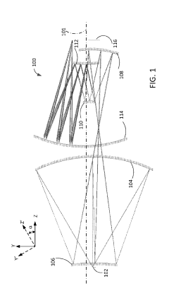
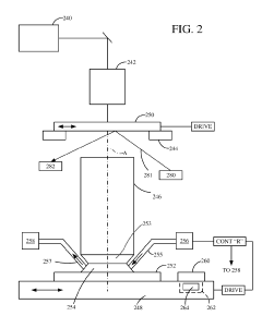
EUV mirror and optical system comprising EUV mirror
PatentWO2014108256A1
Innovation
- A multilayer EUV mirror design featuring three periodic layer groups with specific period thicknesses, where the first and second groups are strictly periodic and the third group introduces a phase shift to reduce reflectivity variation, allowing for a broader usable angle-of-incidence range with reduced production complexity.
High na (numerical aperture) rectangular field EUV catoptric projection optics using tilted and decentered zernike polynomial mirror surfaces
PatentInactiveUS20190113723A1
Innovation
- A catoptric optical system with a plurality of reflective surfaces along a common axis, each offset and tilted symmetrically about a meridian plane, using freeform surfaces like fringe Zernike polynomial-based mirrors to achieve a high numerical aperture of at least 0.5, minimizing aberrations and obliquity effects by maintaining a non-telecentric entrance pupil and reducing off-axis field distances.
Supply Chain Considerations for High-NA EUV Materials
The global supply chain for High-NA EUV materials represents a complex ecosystem that requires careful management to ensure the successful implementation of sub-10 nm half-pitch lithography technologies. The materials required for High-NA EUV lithography include specialized photoresists, pellicles, masks, and various chemicals that must meet extremely stringent purity and performance specifications.
Critical raw material sourcing presents a significant challenge, with rare earth elements and specialized chemicals often concentrated in specific geographic regions. This geographic concentration creates potential supply vulnerabilities, particularly as geopolitical tensions increase. For example, fluorinated compounds essential for photoresist development are primarily produced in a limited number of facilities worldwide, creating potential bottlenecks.
Manufacturing capacity constraints further complicate the supply chain landscape. The production of High-NA EUV materials requires specialized equipment and cleanroom environments that few manufacturers can provide at the necessary scale. Current global capacity for these specialized materials may be insufficient to meet projected demand as High-NA EUV adoption accelerates across the semiconductor industry.
Quality control and consistency represent another critical dimension of the supply chain challenge. Even minor variations in material properties can significantly impact lithographic performance at sub-10 nm dimensions. This necessitates advanced metrology systems throughout the supply chain and close collaboration between material suppliers and end users to establish robust quality assurance protocols.
Transportation and storage logistics add another layer of complexity. Many High-NA EUV materials have limited shelf lives and require specialized handling conditions, including temperature and humidity control. The global nature of the semiconductor supply chain means these sensitive materials must often travel significant distances while maintaining their critical properties.
Risk mitigation strategies are increasingly important given these challenges. Leading semiconductor manufacturers are pursuing multi-sourcing agreements, investing in strategic stockpiles, and even considering vertical integration for critical materials. Additionally, research into alternative materials that could reduce dependence on scarce resources is accelerating, though such alternatives must still meet the exacting performance requirements of High-NA EUV lithography.
Regulatory compliance across different jurisdictions further complicates the supply chain. Many High-NA EUV materials are subject to strict environmental regulations, export controls, and safety requirements that vary by country. Navigating this complex regulatory landscape requires significant resources and expertise, potentially limiting the number of viable suppliers.
Environmental Impact and Sustainability of Advanced Lithography
The advancement of High-NA EUV lithography technology towards sub-10 nm half-pitch manufacturing brings significant environmental and sustainability considerations that must be addressed by the semiconductor industry. The environmental footprint of advanced lithography systems extends beyond their operational phase to include manufacturing, transportation, and end-of-life disposal.
Energy consumption represents one of the most critical environmental concerns in EUV lithography. High-NA EUV systems require substantial power inputs, with current systems consuming between 500-1000 kW during operation. This energy demand necessitates comprehensive efficiency improvements and potential integration with renewable energy sources to mitigate carbon emissions associated with semiconductor manufacturing facilities.
Water usage presents another substantial environmental challenge. The production of EUV lithography systems and their operation in cleanroom environments requires ultra-pure water in significant quantities. A typical semiconductor fabrication facility utilizing advanced lithography may consume 2-4 million gallons of water daily. Innovations in water recycling systems and closed-loop water management have become essential sustainability initiatives across the industry.
Chemical consumption and waste management constitute additional environmental concerns. High-NA EUV processes utilize specialized photoresists, developers, and cleaning agents that may contain potentially hazardous substances. The industry has been progressively transitioning toward more environmentally benign alternatives, with recent developments focusing on metal-free photoresists and biodegradable developers that maintain the necessary performance characteristics for sub-10 nm patterning.
Material resource efficiency has emerged as a priority in sustainable lithography development. The rare earth elements and specialized materials required for EUV mirrors, masks, and supporting equipment face potential supply constraints. Leading equipment manufacturers have implemented comprehensive recycling programs for critical components, particularly the expensive multilayer mirrors used in EUV optical systems.
Regulatory compliance frameworks continue to evolve globally, with initiatives like the EU's Restriction of Hazardous Substances (RoHS) directive and various international agreements on greenhouse gas emissions directly impacting lithography technology development. Companies pursuing High-NA EUV technology must navigate an increasingly complex regulatory landscape while maintaining technological progress toward sub-10 nm nodes.
Industry consortia including SEMI and the Semiconductor Climate Consortium have established roadmaps for environmental sustainability that parallel technological development roadmaps. These collaborative efforts aim to reduce the environmental impact of advanced lithography while maintaining the pace of innovation required by Moore's Law and beyond.
Unlock deeper insights with Patsnap Eureka Quick Research — get a full tech report to explore trends and direct your research. Try now!
Generate Your Research Report Instantly with AI Agent
Supercharge your innovation with Patsnap Eureka AI Agent Platform!