Semiconductor device including channel structure

a technology of a channel structure and a semiconductor device, which is applied in the direction of semiconductor devices, basic electric elements, electrical appliances, etc., can solve the problem of a large number of process defects, and achieve the effect of increasing the degree of integration

Active Publication Date: 2018-06-12
SAMSUNG ELECTRONICS CO LTD
View PDF17 Cites 8 Cited by
  • Summary
  • Abstract
  • Description
  • Claims
  • Application Information

AI Technical Summary

Benefits of technology

[0005]An aspect of the present inventive concept may provide a semiconductor device having an increased degree of integration.

Problems solved by technology

When such a channel hole is formed to be relatively small, a greater number of process defects may occur.

Method used


Image

  • Semiconductor device including channel structure
  • Semiconductor device including channel structure
  • Semiconductor device including channel structure

Examples


Embodiment Construction

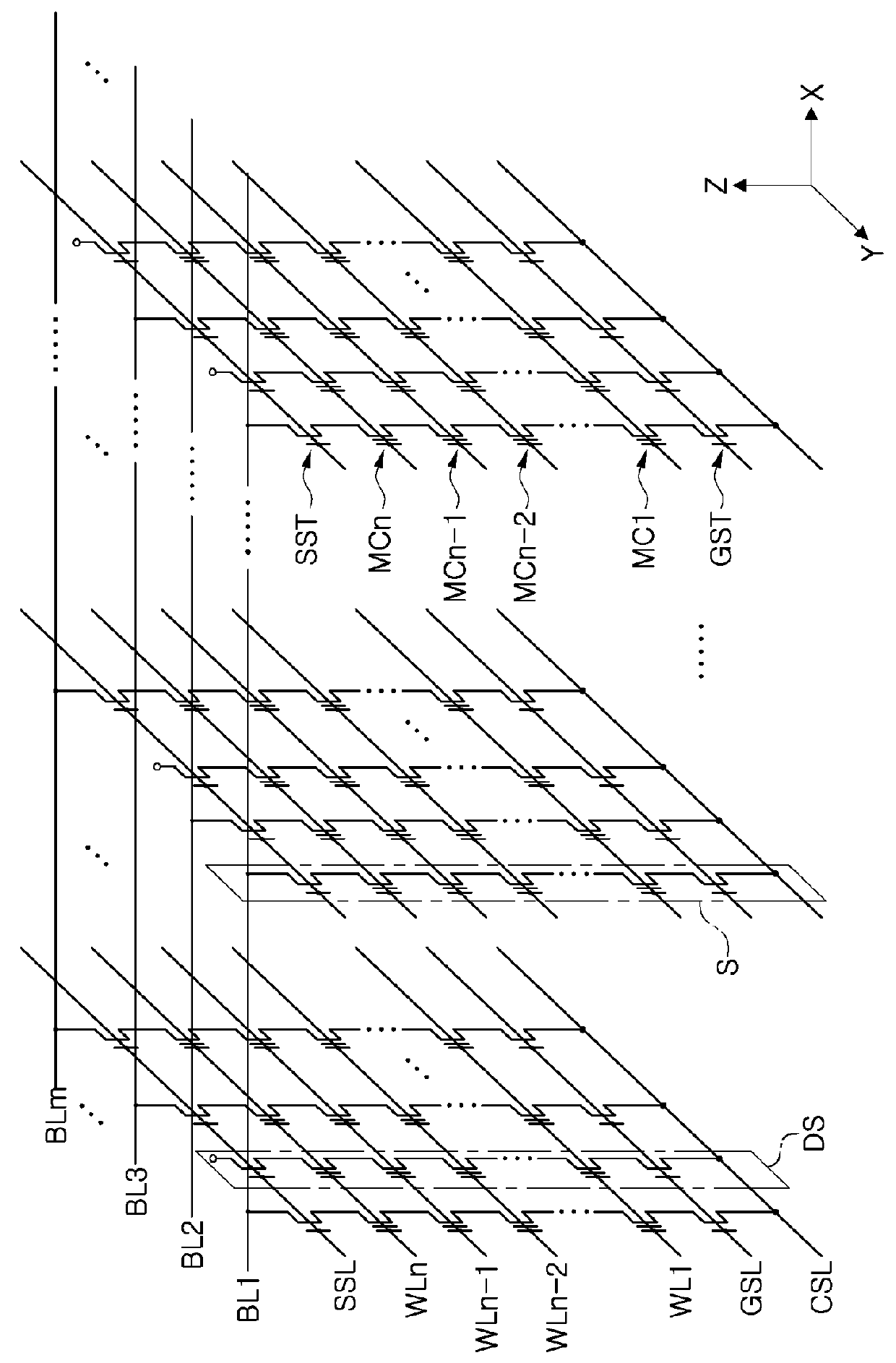
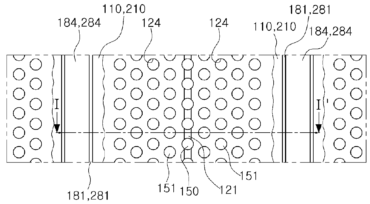
[0021]In the drawings, the size and relative sizes of layers and regions may be exaggerated for clarity. Like numbers refer to like elements throughout. Though the different figures show variations of exemplary embodiments, and may be referred to using language such as “in one embodiment,” these figures are not necessarily intended to be mutually exclusive from each other. Rather, as will be seen from the context of the detailed description below, certain features depicted and described in different figures can be combined with other features from other figures to result in various embodiments, when taking the figures and their description as a whole into consideration.

[0022]It will be understood that, although the terms first, second, third etc. may be used herein to describe various elements, components, regions, layers and / or sections, these elements, components, regions, layers and / or sections should not be limited by these terms. Unless the context indicates otherwise, these te...


PUM


Abstract

A semiconductor device includes a stacked structure disposed on a semiconductor substrate. The stacked structure includes interlayer insulating layers and gate electrodes, alternately stacked. Separation patterns are disposed to penetrate the stacked structure. A channel structure is disposed between the separation patterns. The channel structure includes a horizontal portion interposed between the stacked structure and the semiconductor substrate while being in contact with the semiconductor substrate and includes vertical portions extending from the horizontal portion in a vertical direction and penetrating the stacked structure. A lower structure is interposed between the horizontal portion and the separation patterns. A dielectric structure is interposed between the vertical portions and the stacked structure and extends between the horizontal portion and the stacked structure.

Description

CROSS-REFERENCE TO RELATED APPLICATION[0001]This application claims benefit of priority to Korean Patent Application No. 10-2016-0147361 filed on Nov. 7, 2016 in the Korean Intellectual Property Office, the disclosure of which is incorporated herein by reference in its entirety.BACKGROUND1. Field[0002]The present disclosure relates to a semiconductor device including a channel structure and a method of forming the same.2. Description of Related Art[0003]In order to increase the degree of integration of semiconductor devices, semiconductor devices including three-dimensional vertical transistors, rather than two-dimensional planar transistors, have been proposed. In general, vertical NAND (V-NAND) flash memory devices include a plurality of gate electrodes, as well as gate insulating layers and channel layers formed in a channel hole penetrating through the plurality of gate electrodes in a vertical direction. The channel layers may be in contact with an epitaxial layer formed by bei...

Claims


Application Information

Patent Timeline
Patent Type & Authority Patents(United States)
IPC IPC(8): H01L27/115H01L27/11582
CPCH01L27/11582H10B41/27H10B43/27H10B43/10H01L29/732H01L29/66666H01L29/1025H01L29/6656H01L29/6675
Inventor SON, YONG HOONKIM, YOON JAENAM, SEOK WOO
Owner SAMSUNG ELECTRONICS CO LTD
Why Eureka
Try Eureka