Biscarbazole derivative host materials and green emitter for OLED emissive region
a technology of oled emissive region and host material, which is applied in the field of organic electroluminescent devices, can solve the problems of cbp being known to have a very short life, unsuitable for practical use, and cbp being heavily deteriorated, and achieves low voltage requirements, improved device life, and high luninous efficiency
- Summary
- Abstract
- Description
- Claims
- Application Information
AI Technical Summary
Benefits of technology
Problems solved by technology
Method used
Image

Examples
first embodiment
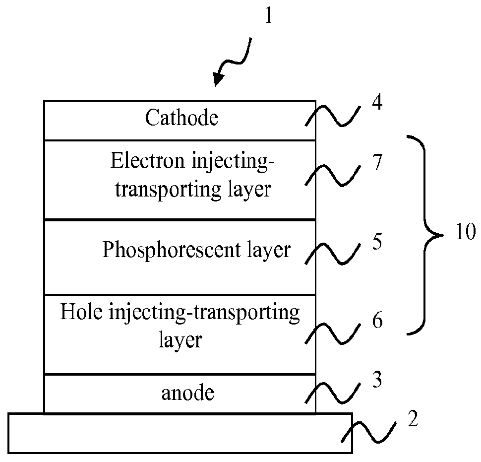
[Light Emitting Layer ]
[0099]The light emitting layer in the OLED of the present disclosure may be capable of carrying out the following functions singly or in combination:[0100](1) injecting function: a function in which a hole can be injected from an anode or a hole injecting layer in applying an electric field and in which an electron can be injected from a cathode or an electron injecting layer;[0101](2) transporting function: a function in which a charge (electron and hole) injected may be transferred by virtue of a force of an electric field; and[0102](3) light emitting function: a function in which a region for recombination of an electron and a hole may be provided, and which results in the emission of light.
[0103]A difference may be present between ease of injection of a hole and ease of injection of an electron, and a difference may be present in the transporting ability shown by the mobilities of a hole and an electron.
[0104]Known methods including, for example, vapor dep...
second embodiment
[Light Emitting Layer ]
[0182]According to another embodiment, an organic EL device comprises a cathode, an anode, and a plurality of organic thin-film layers provided between the cathode and the anode and at least one of the plurality of organic thin-film layers comprise an emitting layer comprising a first host material, a second host material, and a green phosphorescent dopant material as emitter. The first host material of the pair of co-host materials is a biscarbazole derivative compound represented by formula (1A) or (1B) as described.
[0183]
[0184]A second host material of the pair of co-host materials is a biscarbazole derivative compound represented by a formula (1A′), (1B′) or (2) below:
[0185]
wherein A1′ represents a substituted or unsubstituted nitrogen-containing heterocyclic group having 1 to 30 carbon atoms forming a ring;
[0186]A2′ represents a substituted or unsubstituted aromatic hydrocarbon group having 6 to 30 ring carbon atoms, or substituted or unsubstituted nitrog...
PUM
| Property | Measurement | Unit |
|---|---|---|
| quantum efficiency | aaaaa | aaaaa |
| quantum efficiency | aaaaa | aaaaa |
| internal quantum efficiencies | aaaaa | aaaaa |
Abstract
Description
Claims
Application Information
 - R&D
- Intellectual Property
- Life Sciences
- Materials
- Tech Scout
- Unparalleled Data Quality
- Higher Quality Content
- 60% Fewer Hallucinations
Browse by: Latest US Patents, China's latest patents, Technical Efficacy Thesaurus, Application Domain, Technology Topic, Popular Technical Reports.
© 2025 PatSnap. All rights reserved.Legal|Privacy policy|Modern Slavery Act Transparency Statement|Sitemap|About US| Contact US: help@patsnap.com