Layout of semiconductor device

Active Publication Date: 2018-02-20
UNITED MICROELECTRONICS CORP
View PDF7 Cites 0 Cited by
  • Summary
  • Abstract
  • Description
  • Claims
  • Application Information

AI Technical Summary

Benefits of technology

The present invention provides a new way to layout a semiconductor device, like an inverter, that reduces the number of plugs needed and allows for more flexible arrangement. By using a conductive layer in a pre-plug level to form part of the interconnection system, the entire layout of the device can be shrunk by more than 20%. Plugs can also be formed partially overlapping with diffusion regions, which simplifies the cell size and reduces the need for plug structure in alignment with gates.

Problems solved by technology

It is found that valuable areas in the elements with cells of multi-heights are always wasted and complexities of circuit design and manufacturing processes are both increased.

Method used


Image

  • Layout of semiconductor device
  • Layout of semiconductor device
  • Layout of semiconductor device

Examples


Embodiment Construction

[0015]To provide a better understanding of the present invention, preferred embodiments will be described in detail. The preferred embodiments of the present invention are illustrated in the accompanying drawings with numbered elements.

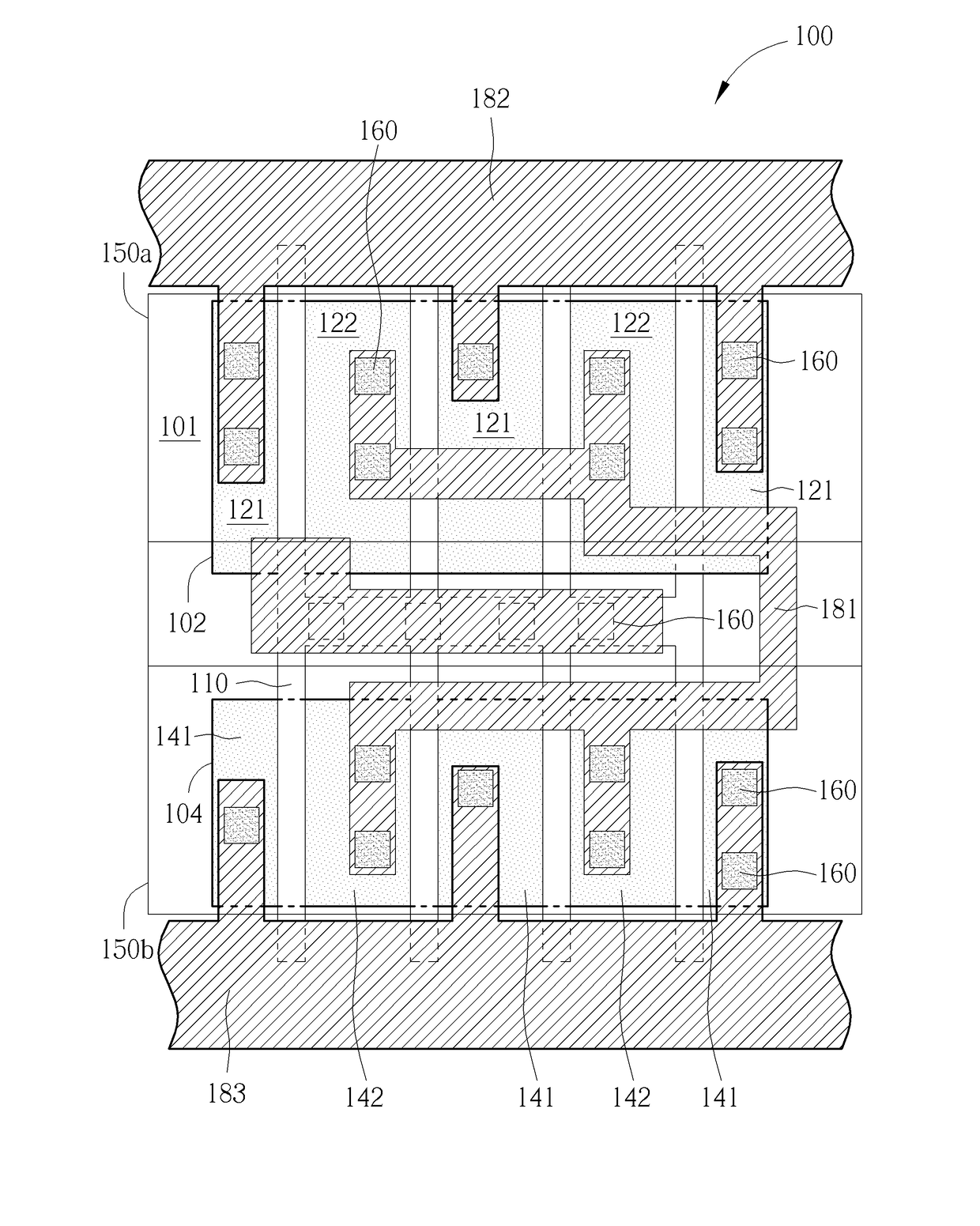
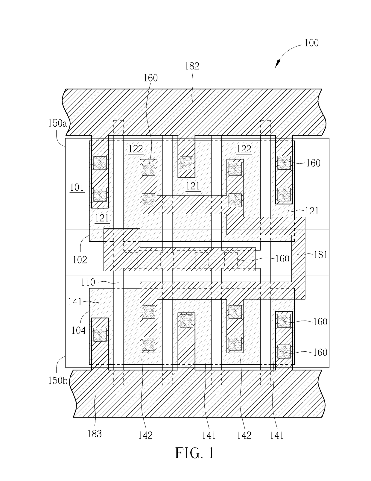
[0016]Referring to FIG. 1, FIG. 1 shows a layout of a semiconductor device according to the first preferred embodiment of the present invention. At first, a semiconductor substrate (not shown in the drawings) is provided, and an active area (AA) 102, an AA 104 and a shallow trench isolation (STI) region 101 surrounded the AAs 102, 104 are formed thereon. In one embodiment, the semiconductor substrate for example includes a silicon substrate, silicon containing substrate (such as SiC or SiGe) or a silicon on insulator (SOI) substrate, but is not limited thereto.

[0017]At least one gate 110 is disposed on the semiconductor substrate and is extended along a first direction such as a y-direction, to simultaneously cross the AAs 102, 104, as shown in FIG. 1...


PUM


Abstract

A layout of a semiconductor device includes a first active area, a second active area, plural gates, a first conductive layout and plural plugs. The first and the second active areas are disposed on a substrate and surrounded by a shallow trench isolation (STI). The plural gates are parallel with one another and cross the first and the second active areas. The first conductive layer covers the plural gates, and the plural gates are electrically connected to each other through the first conductive layer. The plural plugs are disposed on the first conductive layer to electrically connect the plural gates.

Description

BACKGROUND OF THE INVENTION1. Field of the Invention[0001]The present invention relates generally to a layout of a semiconductor device and more particularly, to a layout of an inverter.2. Description of the Prior Art[0002]Semiconductor integrated circuits are one of the most important hardware bases in the modern information society. A key design point of the semiconductor industry is to increase integration of integrated circuits, and therefore to use the area of integrated circuits more efficiently.[0003]Generally speaking, integrated circuits having complex functions are made up of many standard cells, each with basic functions. For example, standard cells of different kinds of logic gates, such as AND gates, OR gates, NOR gates, inverters, cells of flip-flops, adders and counters, are always used to realize complex integrated circuits.[0004]It is found that valuable areas in the elements with cells of multi-heights are always wasted and complexities of circuit design and manufa...

Claims


Application Information

Patent Timeline
IPC IPC(8): H01L23/528H01L27/02H01L27/092H01L29/06H01L23/535
CPCH01L27/0207H01L27/092H01L29/0653H01L23/535H01L21/823828H01L21/823871H01L27/11807H01L2027/11875
Inventor ZHOU, ZHIBIAOCHEN, DING-LUNG
Owner UNITED MICROELECTRONICS CORP
Why Eureka
Try Eureka