
Integrated coherent receiver having a geometric arrangement for improved device efficiency

a technology of integrated coherent receiver and geometric arrangement, applied in the field of integrated coherent receiver chip, can solve the problems of reducing chip size and propagation loss, and achieve the effect of efficient and reliable assembly process

Active Publication Date: 2017-11-07
O NET COMM (SHENZHEN) LTD
View PDF5 Cites 0 Cited by
  • Summary
  • Abstract
  • Description
  • Claims
  • Application Information

AI Technical Summary

Benefits of technology

[0021]The present invention proposes a unique architecture for an integrated coherent receiver chip used for applications using DP-QPSK and higher coherent optical modulation formats. It overcomes the issues of the prior art and provides an integrated coherent chip suitable for a hybrid coherent receiver module which not only meets all performance requirements but also enables efficient and reliable assembly processes.
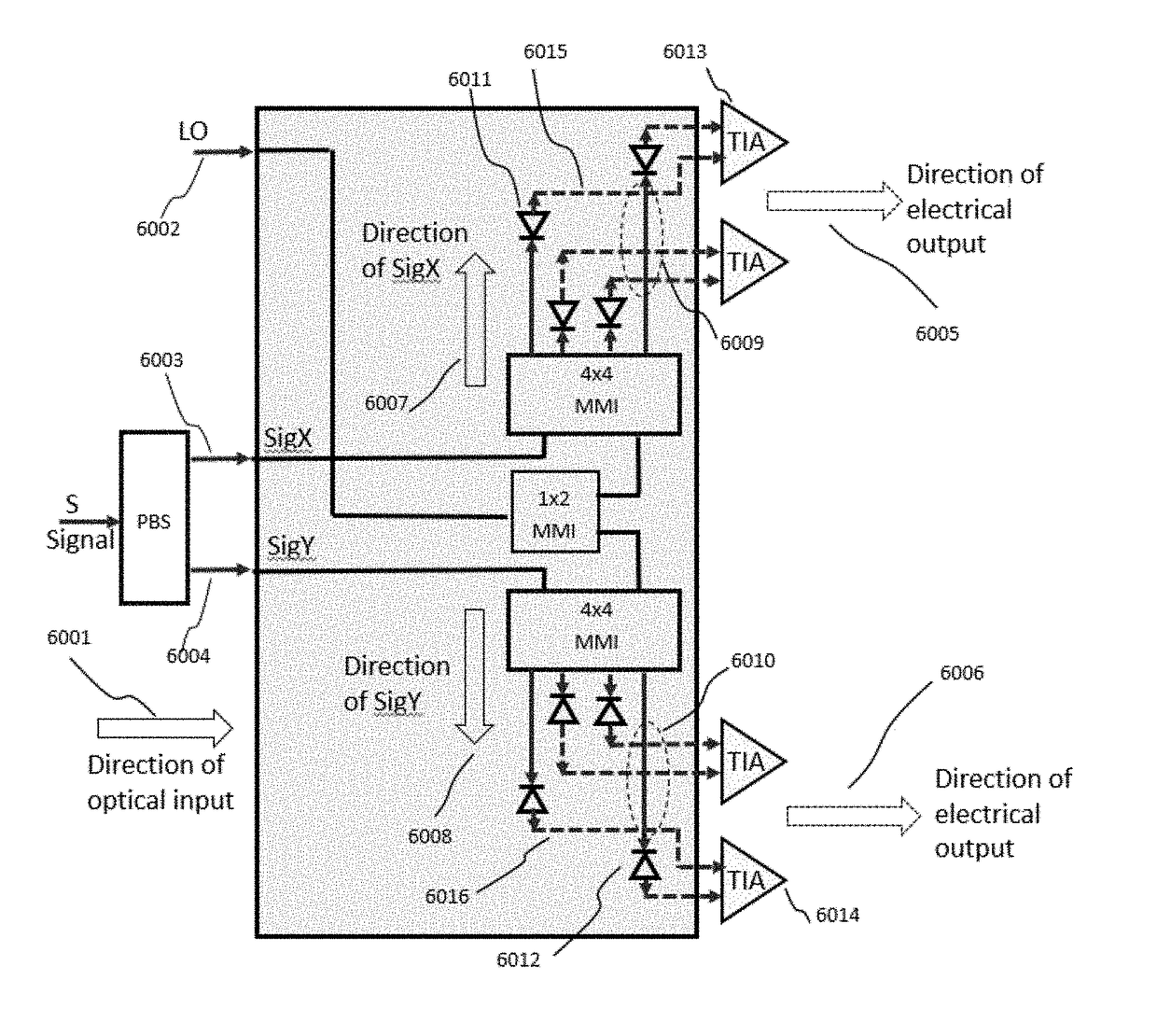
[0022]The first embodiment of the proposed architecture is a coherent receiver chip, which integrates items (1)-(4), as depicted in FIG. 6. The core of this receiver chip is a photonics integrated chip (PIC) which has two optical hybrids, eight high speed waveguide photo-detectors (WPD) with on-chip bias circuitry. The geometric arrangement of the proposed architecture directs the optical axes of the 90° hybrids parallel to the input optical facet. The benefits of this arrangement are threefold. First, it widens the chip and provides the space to spread the three optical inputs so that the separation of SigX and SigY can readily be adjusted to match the requirements of the PBS. Moreover, the LO can be remote from the signal pair at the chip facet and yet routed between the SigX and SigY paths, where it is split and then fed into each of the two hybrids. This arrangement separates the LO and the signal attachment processes, and thereby greatly improves the efficiency and quality of the input optical coupling as well as enables reliable and high yield module fabrication.
[0023]The second benefit of the proposed architecture, wherein the optical axes of the 90° hybrids are oriented parallel to the input facet, is that the waveguide outputs of the hybrid can be directed to the corresponding electrical outputs without any optical waveguide crossings and yet maintaining a co-linear configuration of the optical inputs and the electrical outputs. Here the connections between the optical hybrids and the electrical outputs are made by optical waveguides and electrical transmission lines using vertically integrated electrical-optical crossings instead of optical waveguide crossings, resulting in reduced chip size and propagation loss. This arrangement also adds the flexibility to balance the optical delays with the electrical delays so that the net total delay difference, between the I and Q channels and between photodetector pairs, is minimized. Furthermore, the skew compensation between the two polarizations (SigX and SigY) is facilitated by re-ordering the waveguide inputs to the optical hybrids such that the connections between the optical hybrid and electrical outputs can be mirrored.
[0024]A third advantage of the proposed architecture is that the arrangement also allows wide separation of the electrical outputs, which results in better module thermal management and easy electrical connections. In addition, the proposed architecture enables a variable chip aspect ratio for different packaging needs, i.e. a wider chip width in exchange for a shorter length.
[0026]In the embodiment of FIG. 7, the optical axes of the 90° hybrids can also be oriented perpendicular to the input facet while keeping the waveguide photodetectors parallel, or at a small angle (up to 15°), to the input facet. Such an arrangement provides more flexibility in the locations of the four electrical outputs of X-polarization relative to that of Y-polarization, including a side by side configuration to accommodate a Quad-Trans-Impedance Amplifier.
[0028]In another embodiment of the chip architectural arrangement, the compactness and the functions of the chip can be further enhanced by having an array of two or more coherent receivers integrated on a single chip, wherein the LO can be shared between all receivers. FIG. 9 shows an exemplary configuration of such a device wherein two coherent receivers are integrated. This arrangement doubles the information capacity of the coherent receiver chip by allowing integration of two separate signal channels.

Problems solved by technology

Here the connections between the optical hybrids and the electrical outputs are made by optical waveguides and electrical transmission lines using vertically integrated electrical-optical crossings instead of optical waveguide crossings, resulting in reduced chip size and propagation loss.

Method used


Image

  • Integrated coherent receiver having a geometric arrangement for improved device efficiency
  • Integrated coherent receiver having a geometric arrangement for improved device efficiency
  • Integrated coherent receiver having a geometric arrangement for improved device efficiency

Examples


Embodiment Construction

[0042]Preferred embodiments of the present invention will be described below with reference to FIGS. 1-9. It is instructive to start the description with a review of the previous art.

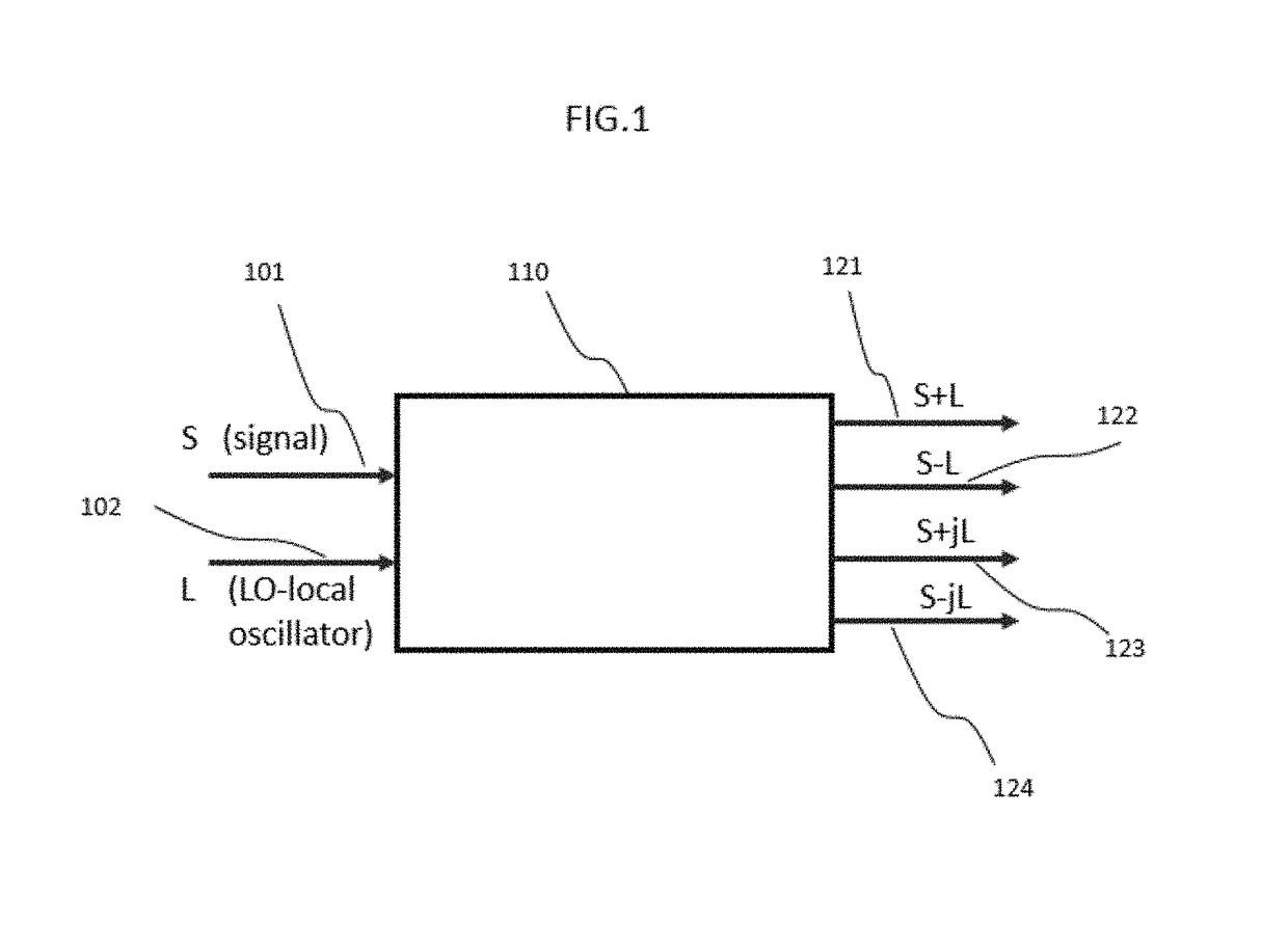
[0043]FIG. 1 presents a schematic view of a generic 90° hybrid with two inputs: the signal S 101 and the local oscillator field L 102 are launched into the mixer 110 where both fields interfere and appear at the output of the MMI as in-phase components S+L 121 and S−L 122, and quadrature components S+jL 123 and S−jL 124.

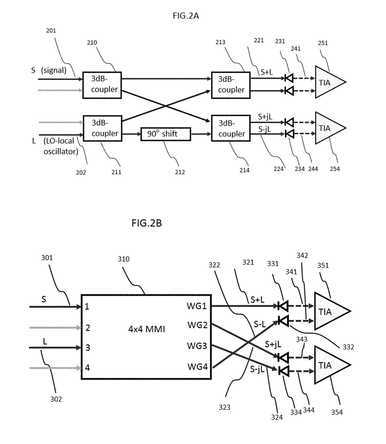
[0044]FIG. 2A illustrates the situation where the hybrid is implemented by means of waveguide mode interference coupler which comprises four 3 dB couplers 210211213214 and a 90° phase shift 212. At the output of the hybrid the optical signals, marked as 221, 224, are directed into photodetectors 231, 224, where the light is detected and transformed into electrical signals 241, 244 which are directed into the TIAs 251, 254.

[0045]FIG. 2B presents the hybrid in the form of 4×4 MMI coupler 3...


PUM


Abstract

Disclosed herein is a monolithically integrated coherent receiver chip which has a geometric arrangement of the on-chip components that significantly improves the performance and the manufacturability of a coherent receiver module for Dual Polarization Quadrature Phase Shift Keyed (DP-QPSK) applications and other optical coherent detection systems. The coherent receiver chip comprises two optical hybrids, three optical inputs and eight electrical outputs with the two optical hybrids oriented perpendicular to the optical inputs and the electrical outputs which are widely spaced and arranged in a co-linear fashion that simplifies module design and assembly. The proposed geometric arrangement also replaces any optical waveguide crossings with vertical electrical-optical crossings and includes electrical transmissions which are used to minimize channel skew. The proposed configuration also has the additional benefit of improved thermal management by separating the module's trans-impedance amplifiers.

Description

CROSS REFERENCE TO RELATED APPLICATIONS[0001]This application claims priority to U.S. provisional application Nos. 62 / 136,830, entitled “INTEGRATED COHERENT RECEIVER CHIP HAVING A GEOMETRIC ARRANGEMENT FOR IMPROVED DEVICE EFFICIENCY,” filed Mar. 23, 2015, and 62 / 136,976, entitled “INTEGRATED COHERENT RECEIVER CHIP HAVING A GEOMETRIC ARRANGEMENT FOR IMPROVED DEVICE EFFICIENCY,” filed Mar. 23, 2015, which are both herein incorporated by reference.FIELD OF THE INVENTION[0002]The invention is related to an integrated coherent receiver chip to be used in coherent receiver module for the applications using Dual Polarization Quadrature Phase Shift Keyed (DP-QPSK) modulation format, or other higher degree modulation formats.BACKGROUND OF THE INVENTION AND PRIOR ART[0003]A coherent receiver module is used in a transmission system adopting dual polarization and quadrature phase-shifted keying modulation format (DP-QPSK). By transmitting 2 bits per symbol on orthogonal polarizations this modul...

Claims


Application Information

Patent Timeline
Patent Type & Authority Patents(United States)
IPC IPC(8): H04B10/61G02B6/30G02B6/42H04B10/25G02B6/28
CPCH04B10/61G02B6/305G02B6/4206G02B6/428H04B10/25G02B6/4295G02B6/4286G02B6/2813G02B6/4213H04B10/613H04B10/614
Inventor WU, FANGTANG, YONGBOLOGVIN, YURYWATSON, CHRISTOPHER D.PIMENOV, KIRILL Y.
Owner O NET COMM (SHENZHEN) LTD
Learn More