Method for manufacturing quantum dot color filter

a color filter and quantum dot technology, applied in the field of display technology, can solve the problems of difficult development of quantum dot photoresists, complex process, and inability to disclose the patterning methods of quantum dots, so as to improve manufacturing efficiency, simplify the process, and reduce the cost

Active Publication Date: 2017-10-31
TCL CHINA STAR OPTOELECTRONICS TECH CO LTD
View PDF3 Cites 2 Cited by
  • Summary
  • Abstract
  • Description
  • Claims
  • Application Information

AI Technical Summary

Benefits of technology

[0007]An object of the present invention is to provide a method for manufacturing a quantum dot color filter, which saves one round of photolithographic operation, simplifying the process, reducing cost, improving manufacturing efficiency, and lowering the difficult and cost for development of quantum dot photoresists.
[0036]The efficacy of the present invention is that the present invention provides a method for manufacturing a quantum dot color filter. The method for manufacturing a quantum dot color filter of the present invention, after forming a blue sub-pixel part of a quantum dot color filter by applying a photolithographic operation to a transparent organic photoresist material, applies hydrophobicity treatment to the transparent organic photoresist layer so as to make use of hydrophobic characteristics so formed to help coat green quantum dot curable paste and red quantum dot photoresist sequentially on corresponding areas to form, in sequence, a green quantum dot curable paste layer and a red quantum dot photoresist layer located thereon, and then applies photolithographic operations to subject portions of the red quantum dot photoresist layer to etching for forming a green sub-pixel part and a red sub-pixel part of the quantum dot color filter, whereby compared to the conventional ways of manufacturing a quantum dot color filter, at least one round of photolithographic operation can be saved to greatly simplify the manufacturing process, reduce cost, and improve manufacturing efficiency, and it only needs to develop one type of quantum dot photoresist so as to greatly reduce difficulty and cost of development.

Problems solved by technology

However, such patent documents do not disclose the ways of patterning the quantum dot layers
However, such a process requires the red, green, and blue quantum dots to be mixed with red, green, and blue quantum dot photoresists first and also requires three photolithographic operations, making the process complicated, and it also need to develop red and green quantum dot photoresists at the same time, making the development of quantum dot photoresists difficult.
However, the quantum dot patterns formed with transfer-printing have poor resolution, where edges of the patterns are in a serrated form and the adhering power between the quantum dot layer and the base requires being further improved.
Inkjet printing may also be used to form patterned quantum dot layer and such a method has a severe requirement for the inkjet printing device.
In addition, there is still technical barrier to maintain stability of the drops of ink jet and the precision of printing, making it not possible for use in mass production.

Method used


Image

  • Method for manufacturing quantum dot color filter
  • Method for manufacturing quantum dot color filter
  • Method for manufacturing quantum dot color filter

Examples


Embodiment Construction

[0048]To further expound the technical solution adopted in the present invention and the advantages thereof, a detailed description is given to a preferred embodiment of the present invention and the attached drawings.

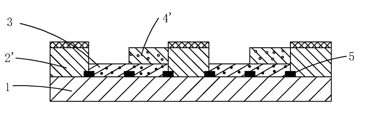
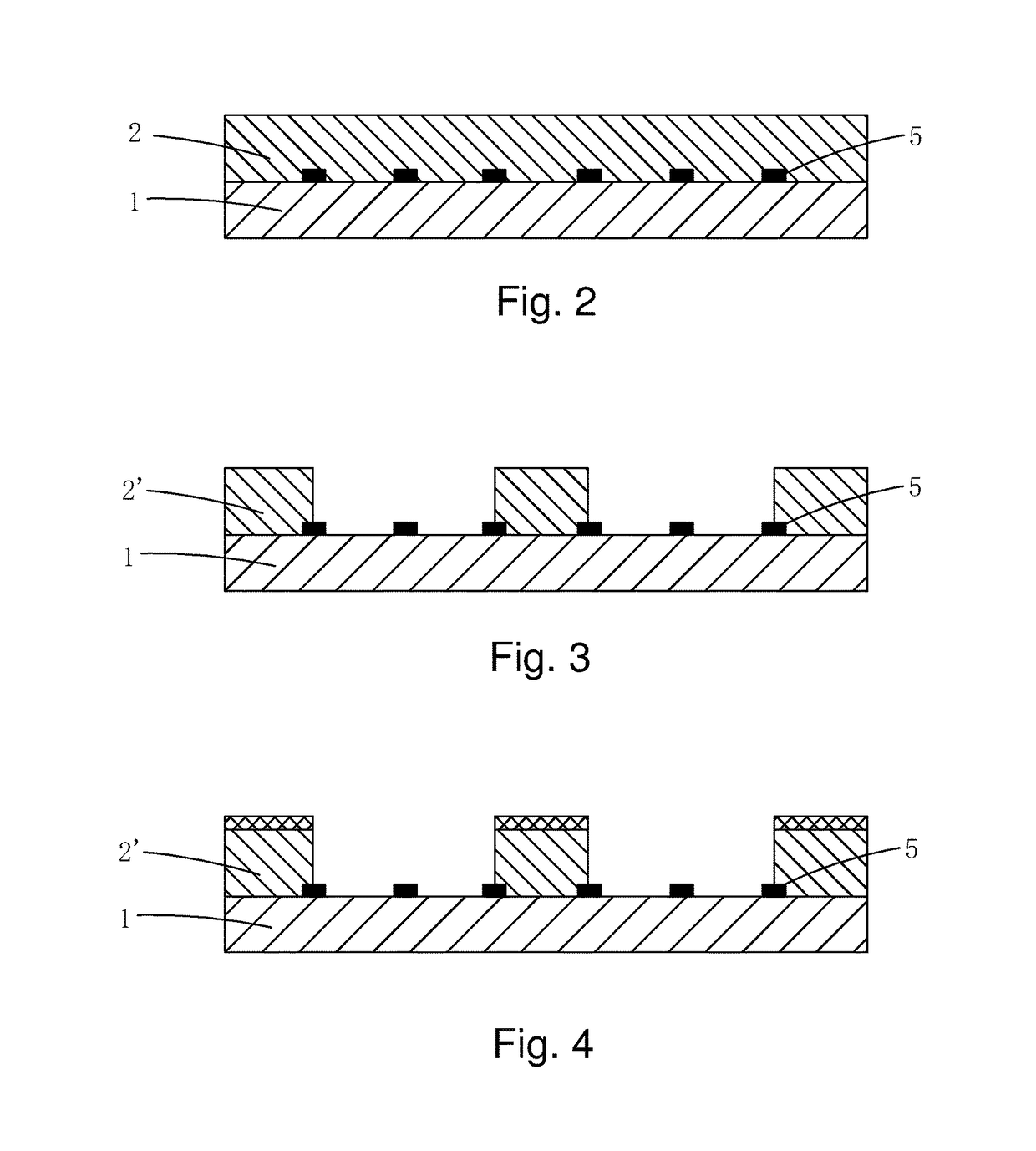
[0049]Referring to FIGS. 1-8, the present invention provides a method for manufacturing a quantum dot color filter, which comprises the following steps:

[0050]Step 1: as shown in FIG. 2, providing a substrate 1, the substrate 1 comprising a plurality of blue sub-pixel zones, green sub-pixel zones, and red sub-pixel zones; and coating a layer of transparent organic photoresist material on the substrate 1 to form a transparent organic photoresist layer 2.

[0051]Specifically, Step 1 further comprises, before coating the layer of transparent organic photoresist material, forming a black matrix 5 on the substrate 1 through a photolithographic operation such that the black matrix 5 separates the blue sub-pixel zones, the green sub-pixel zones, and the red sub-pixel zones from ...


PUM

PropertyMeasurementUnit
thicknessaaaaaaaaaa
luminescence wavelengthaaaaaaaaaa

Abstract

The present invention provides a method for manufacturing a quantum dot color filter. The method for manufacturing a quantum dot color filter of the present invention, after forming a blue sub-pixel part of a quantum dot color filter by applying a photolithographic operation to a transparent organic photoresist material, applies hydrophobicity treatment to the transparent organic photoresist layer so as to make use of hydrophobic characteristics so formed to help coat green quantum dot curable paste and red quantum dot photoresist sequentially on corresponding areas to form, in sequence, a green quantum dot curable paste layer and a red quantum dot photoresist layer located thereon, and then applies photolithographic operations to subject portions of the red quantum dot photoresist layer to etching for forming a green sub-pixel part and a red sub-pixel part of the quantum dot color filter, whereby compared to the conventional ways of manufacturing a quantum dot color filter, at least one round of photolithographic operation can be saved to greatly simplify the manufacturing process, reduce cost, and improve manufacturing efficiency, and it only needs to develop one type of quantum dot photoresist so as to greatly reduce difficulty and cost of development.

Description

BACKGROUND OF THE INVENTION[0001]1. Field of the Invention[0002]The present invention relates to the field of display technology, and in particular to a method for manufacturing a quantum dot color filter.[0003]2. The Related Arts[0004]With the continuous development of the display technology, people increasingly demand higher and higher quality of displaying. Quantum dots (QDs) are nanometer semiconductor particles in the form of spheres or similar to spheres made of elements of II-VI groups or III-V groups, having a particle size between several nanometers and tens of nanometers. Since the particle size of QDs is less than or close to the exciton Bohr radius of the corresponding material, an quantum confinement effect is generally involved, where the energy band structure is changed from quasi-continuity of the body material to the discrete structure of the quantum dot material, making the quantum dots exhibiting unique behavior of stimulated emission of light. When the size of th...

Claims


Application Information

Patent Timeline
Patent Type & Authority Patents(United States)
IPC IPC(8): G02B5/20G02F1/1335G03F7/00
CPCG03F7/0007G02F1/133514G02F2202/36G02B5/207G02F1/133516G02B5/201
Inventor LIANG, YUHENG
Owner TCL CHINA STAR OPTOELECTRONICS TECH CO LTD
Why Eureka
Try Eureka