
Display device

a display device and display technology, applied in non-linear optics, instruments, optics, etc., can solve the problems of not being suitable for low-frequency driving, and achieve the effect of high storage capacitance and not reducing the aperture ratio

Active Publication Date: 2017-10-31
BOE TECH GRP CO LTD
View PDF13 Cites 0 Cited by
  • Summary
  • Abstract
  • Description
  • Claims
  • Application Information

AI Technical Summary

Benefits of technology

The present invention provides a display device that can be driven at both low and high frequencies, while maintaining high aperture ratio without reducing the charge rate during high-frequency driving. By arranging two electrode layers on the substrate, a first capacitor and a second capacitor are formed between them, resulting in a high storage capacitance suitable for low-frequency driving. The electrical connection between the two electrodes is cut off during high-frequency driving to ensure the charge rate, preventing the aperture ratio from being reduced.

Problems solved by technology

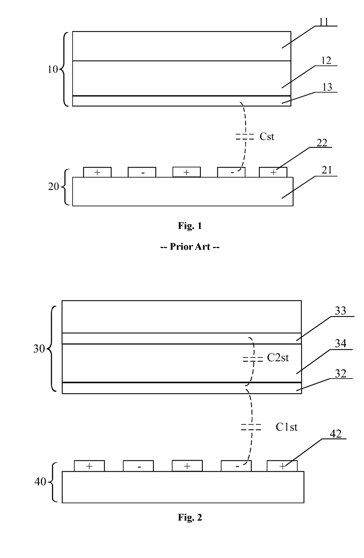
However, when the display device is driven at low frequency (below 30 Hz, generally driven at 10 Hz or 5 Hz), the voltage holding ratio (VHR) depends on the magnitude of the Cst, and if the Cst is too low, the normal value may not be maintained, so relatively high Cst is needed during low-frequency driving.
The novel ADS mode shown in FIG. 1 has an advantage on the aspect of charge rate design during high-frequency driving due to relatively low Cst, but is not suitable for low-frequency driving due to the relatively low Cst.

Method used


Image

  • Display device
  • Display device
  • Display device

Examples


embodiment

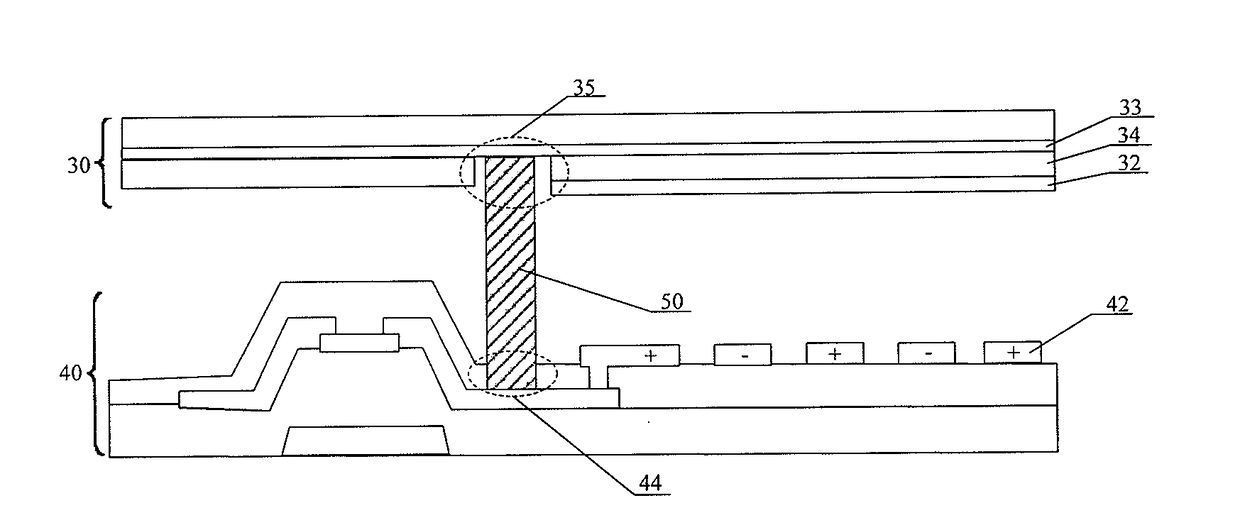
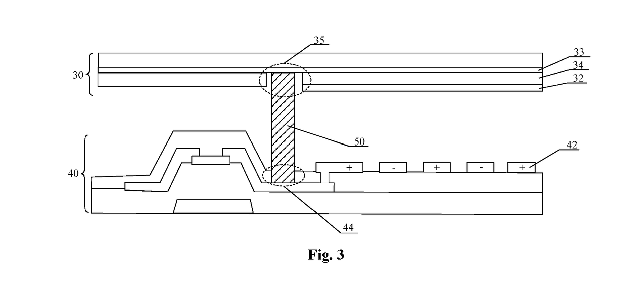
[0032]The embodiment of the present invention provides a display device, as shown in FIG. 2, including a first substrate 30 and a second substrate 40 which are assembled with each other to form a cell, wherein the first substrate 30 includes a first electrode layer 32, the second substrate 40 includes a second electrode layer 42, the first substrate 30 further includes a third electrode layer 33 arranged on one side (namely above the first electrode layer 32), far from the second substrate 40, of the first electrode layer 32, moreover, an insulation layer 34 is arranged between the third electrode layer 33 and the first electrode layer 32, and the third electrode layer 33 is electrically connected with the second electrode layer 42.

[0033]In an existing display device, the first and second electrode layers for generating driving electric fields are respectively positioned on a color filter substrate and an array substrate and are relatively far from each other, and Cst is relatively ...


PUM

PropertyMeasurementUnit
frequencyaaaaaaaaaa
frequencyaaaaaaaaaa
frequencyaaaaaaaaaa

Abstract

The embodiment of the present invention discloses a display device, which relates to the field of display, may realize low-frequency (low-standing-wave) driving and may prevent the aperture ratio from being reduced as a result of ensuring the charge rate during high-frequency driving. The display device provided by the present invention comprises a first substrate and a second substrate which are assembled with each other to form a cell, wherein the first substrate comprises a first electrode layer, the second substrate comprises a second electrode layer, the first substrate further comprises a third electrode layer arranged on one side, far from the second substrate, of the first electrode layer, and an insulation layer is arranged between the third electrode layer; and the first electrode layer, and the third electrode layer is electrically connected with the second electrode layer. The display device is suitable for being driven at low frequency.

Description

[0001]This is a National Phase Application filed under 35 U.S.C. 371 as a national stage of PCT / CN2014 / 076233, filed Apr. 25, 2014, and claims priority benefit from Chinese Application No. 201310673600.X, filed Dec. 10, 2013, the content of each of which is hereby incorporated by reference in its entirety.FIELD OF THE INVENTION[0002]The present invention relates to the field of display, and particularly relates to a display device.BACKGROUND OF THE INVENTION[0003]Generally, when a display device is driven at high frequency (60 Hz, 120 Hz and the like), high storage capacitance Cst influences the charge rate, so the Cst needs to be designed into a relatively small value. However, when the display device is driven at low frequency (below 30 Hz, generally driven at 10 Hz or 5 Hz), the voltage holding ratio (VHR) depends on the magnitude of the Cst, and if the Cst is too low, the normal value may not be maintained, so relatively high Cst is needed during low-frequency driving. For examp...

Claims


Application Information

Patent Timeline
Patent Type & Authority Patents(United States)
IPC IPC(8): G02F1/1343G02F1/1333G02F1/1335G02F1/1368G02F1/1362G02F1/1339
CPCG02F1/134363G02F1/1368G02F1/133345G02F1/133512G02F1/133514G02F1/134309G02F2202/16G02F1/1339G02F2001/13398G02F2001/134381G02F2001/136222G02F2201/121G02F1/13398G02F1/134381G02F1/136222
Inventor CHOI, HYUNSICKIM, HEECHEOL
Owner BOE TECH GRP CO LTD
Learn More