Manufacturing method for a phase modulation system with ultraviolet discharge of accumulated charges

a phase modulation and manufacturing method technology, applied in the field of optical functional devices, can solve the problems of increasing the size of the plc element and power consumption, increasing the power consumption used to hold control and operation of optical switches, and limitations of functionality and performance achieved by conventional silica-based plcs, etc., to achieve the effect of reducing standby power, saving power, and producing cross-sectional structures

Active Publication Date: 2017-08-08
NEC CORP
View PDF27 Cites 2 Cited by
  • Summary
  • Abstract
  • Description
  • Claims
  • Application Information

AI Technical Summary

Benefits of technology

[0019]The optical functional device of the present invention is designed to change a refractive index of an optical waveguide so as to switch over propagation paths of light-waves and control phase delays. In particular, the present invention aims to save power when holding phase-varied states. Specifically, the present invention demonstrates the following effects.
[0020]According to a first effect, it is possible to change a refractive index of an optical waveguide via electric control while holding the refractive-index changed state without power. Thus, the present invention can freely store and rewrite complex functions, including optical switches, wavelength tunable filters, and optical circuits, while significantly reducing standby power. According to a second effect, it is possible to produce the cross-sectional structure of an optical waveguide via similar manufacturing processes of transistors used in silicon integrated circuits (e.g. flash memory). Thus, it is possible to produce plenty of optical functional devices, according to the present invention, via mature processes of silicon integrated circuits with low cost. According to a third effect, it is possible to produce optical circuits, which can set and erase complex optical function control programs, with a high degree of integration via processes of silicon integrated circuits. According to a fourth effect, it is possible to design an optical function device using the structure of an electric field-effect transistor while achieving charge storage of an optical waveguide by use of hot-carrier injection due to impact ionization. Thus, it is possible to increase the distance between a control electrode (e.g. a gate electrode) and a floating waveguide core while reducing an optical propagation loss due to a reduction of light-wave effusion into a control electrode.

Problems solved by technology

However, due to complex and advanced functions required for optical functional devices, it is necessary to increase the size of PLC elements and power consumption for driving PLC, which in turn causes limitations to functionality and performance achieved by conventional silica-based PLC.
However, it is necessary to increase power consumption used to hold control and operation of optical switches as optical-circuit paths become complex since it is necessary to hold optical-circuit paths applied to optical switches for several days or several months.

Method used


Image

  • Manufacturing method for a phase modulation system with ultraviolet discharge of accumulated charges
  • Manufacturing method for a phase modulation system with ultraviolet discharge of accumulated charges
  • Manufacturing method for a phase modulation system with ultraviolet discharge of accumulated charges

Examples


first embodiment

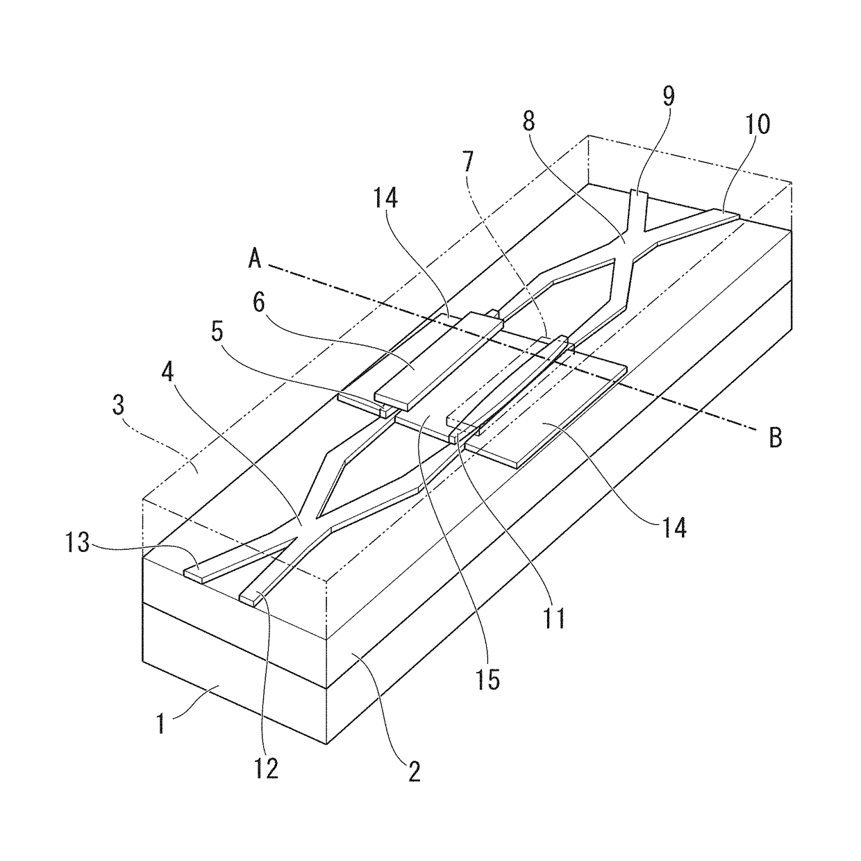
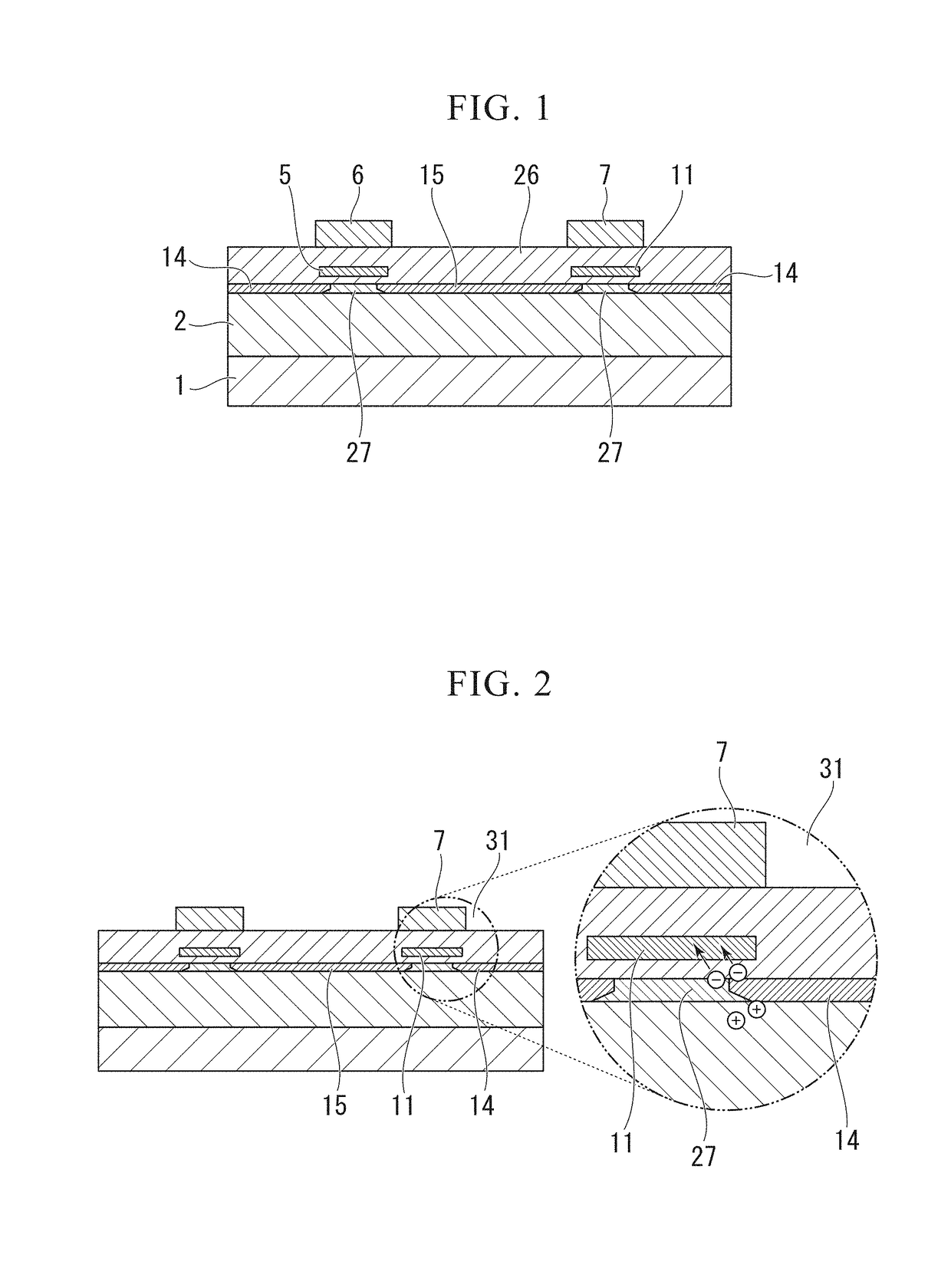
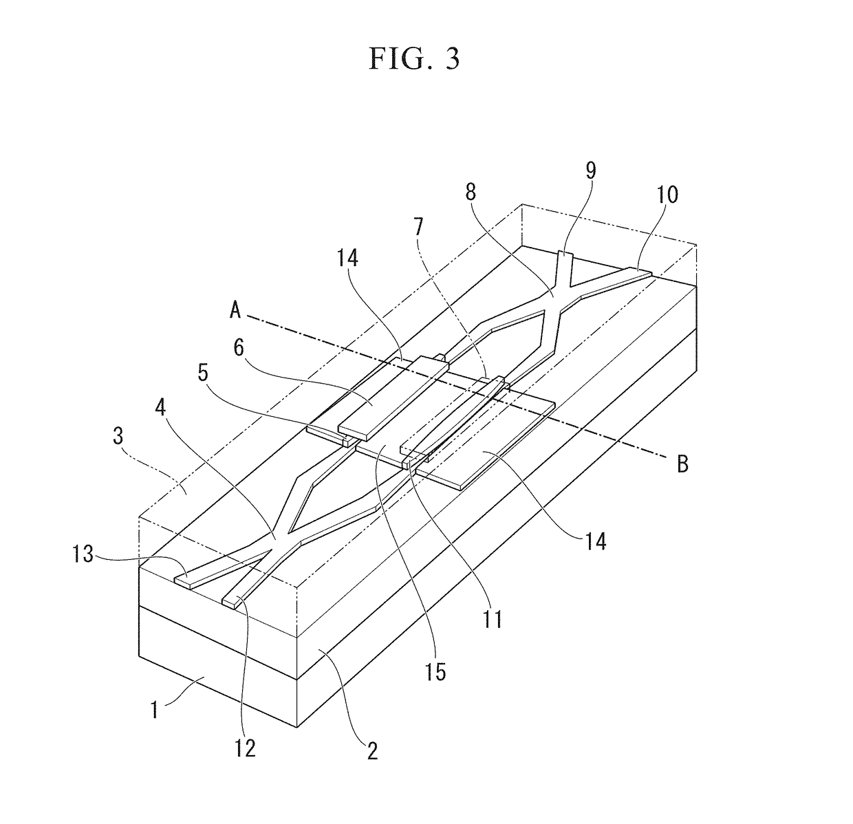
[0030]The optical functional device serving as an optical switch according to the first embodiment of the present invention will be described in detail with reference to FIGS. 1 to 3 and FIGS. 6 to 8. FIG. 3 is a perspective view of the optical switch, while FIGS. 1 and 2 are cross-sectional views taken along line A-B in FIG. 3. FIG. 2 is a partially enlarged cross-sectional view of FIG. 1.

[0031]In the present invention, a substrate is produced by sequentially forming a buried silicon oxide film 2 and an SOI (Silicon On Insulator) layer on a silicon substrate 1. By appropriately processing the SOI layer in the substrate, it is possible to form a 2×2 Mach-Zehnder optical switch including 3 dB MMI (Multi Mode Interference) couplers 4, 8, input waveguides 12, 13, and output waveguides 9, 10. A pair of poly-silicon waveguides (or optical phase modulation paths) used to accumulate charges is formed on a pair of waveguides interposed between the MMI couplers 4 and 8, while a pair of poly-...

second embodiment

[0042]Next, a ring-type wavelength tunable filter serving as an optical functional device according to the second embodiment of the present invention will be described with reference FIGS. 4 and 5. The ring-type wavelength tunable filter includes an electrically-floated waveguide (i.e. a floating waveguide), which is able to accumulate electric charges, at part of a ring-type optical waveguide (or a ring-type wavelength filter). FIG. 4 is a perspective view of the ring-type wavelength tunable filter, while FIG. 5 is a cross-sectional view taken along line C-D in FIG. 4.

[0043]A substrate is produced by sequentially forming a buried silicon oxide film 42 and a SOI layer on a silicon substrate 41. By appropriately processing the SOI layer in the substrate, it is possible to form input / output waveguides 43, 47, 48, 51 as well as a source region 52 and a drain region 53. Impurities are doped into the substrate such that the source region 52 and the drain region 53 will have predetermined...


PUM

PropertyMeasurementUnit
refractive indexaaaaaaaaaa
thicknessaaaaaaaaaa
thicknessaaaaaaaaaa

Abstract

An optical functional device equivalent to a 2×2 Mach-Zehnder optical switch is produced by forming two 3 dB couplers and input / output waveguides on a substrate. Two optical phase modulation paths are formed on corresponding waveguides between 3 dB couplers. A channel region having an opposite electric polarity is formed between source and drain regions, having the predetermined electric polarity, formed on the substrate. The optical phase modulation path is insulated from the surrounding area and disposed above the channel region. Additionally, a control electrode (i.e. a gate region) subjected to high-density doping is formed above the optical phase modulation path. By applying an electric voltage having the predetermined polarity to the control electrode, the source region, and the drain region, it is possible to generate hot carriers, in proximity to the optical phase modulation path, so as to accumulate charges and change a refractive index, thus setting a desired light-wave input / output path.

Description

TECHNICAL FIELD[0001]The present invention relates to an optical functional device, such as a wavelength tunable filter and a nonvolatile optical switch using an optical phase modulation element, and a manufacturing method thereof.[0002]The present application claims priority on Japanese Patent Application No. 2012-79609 filed Mar. 30, 2012, the entire content of which is incorporated herein by reference.BACKGROUND ART[0003]Conventionally, silica-based planar light-wave circuits (PLC) have been developed for practical use, and therefore array waveguide gratings (AWG) and optical splitters have played a key role as key components supporting recent optical communication markets. Recently, optical functional devices such as wavelength tunable light sources hybrid-mounted on semiconductor optical amplifiers (SOA) and silica-based PLC have been developed to achieve an inexpensive small-size system on a single chip by mounting active elements and passive elements on the common PLC substra...

Claims


Application Information

Patent Timeline
Patent Type & Authority Patents(United States)
IPC IPC(8): H04B10/564G02F1/225H04B10/25H04B10/548H04Q11/00G02F1/01G02F1/21
CPCH04B10/564G02F1/2257H04B10/25H04B10/548H04Q11/0005G02F1/0121G02F2001/212G02F2203/055G02F2203/15H04Q2011/0035H04Q2011/0039G02F1/212
Inventor ISHIZAKA, MASASHIGE
Owner NEC CORP
Why Eureka
Try Eureka