Touch panel and liquid crystal display comprising the same
a technology of liquid crystal display and touch panel, which is applied in the field of touch panel and liquid crystal display, can solve the problems of increased thickness of conventional portable communication devices, insufficient satisfaction of users of portable communication devices, and increased space requirements, so as to improve accuracy and sensitivity of touch input, the thickness of the touch panel may not be increased, and the effect of preventing damag
- Summary
- Abstract
- Description
- Claims
- Application Information
AI Technical Summary
Benefits of technology
Problems solved by technology
Method used
Image
Examples
first embodiment
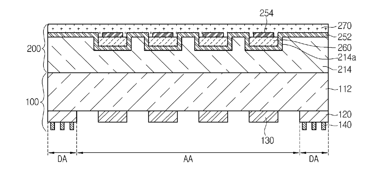
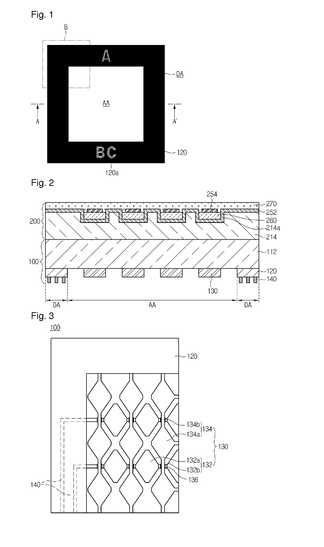
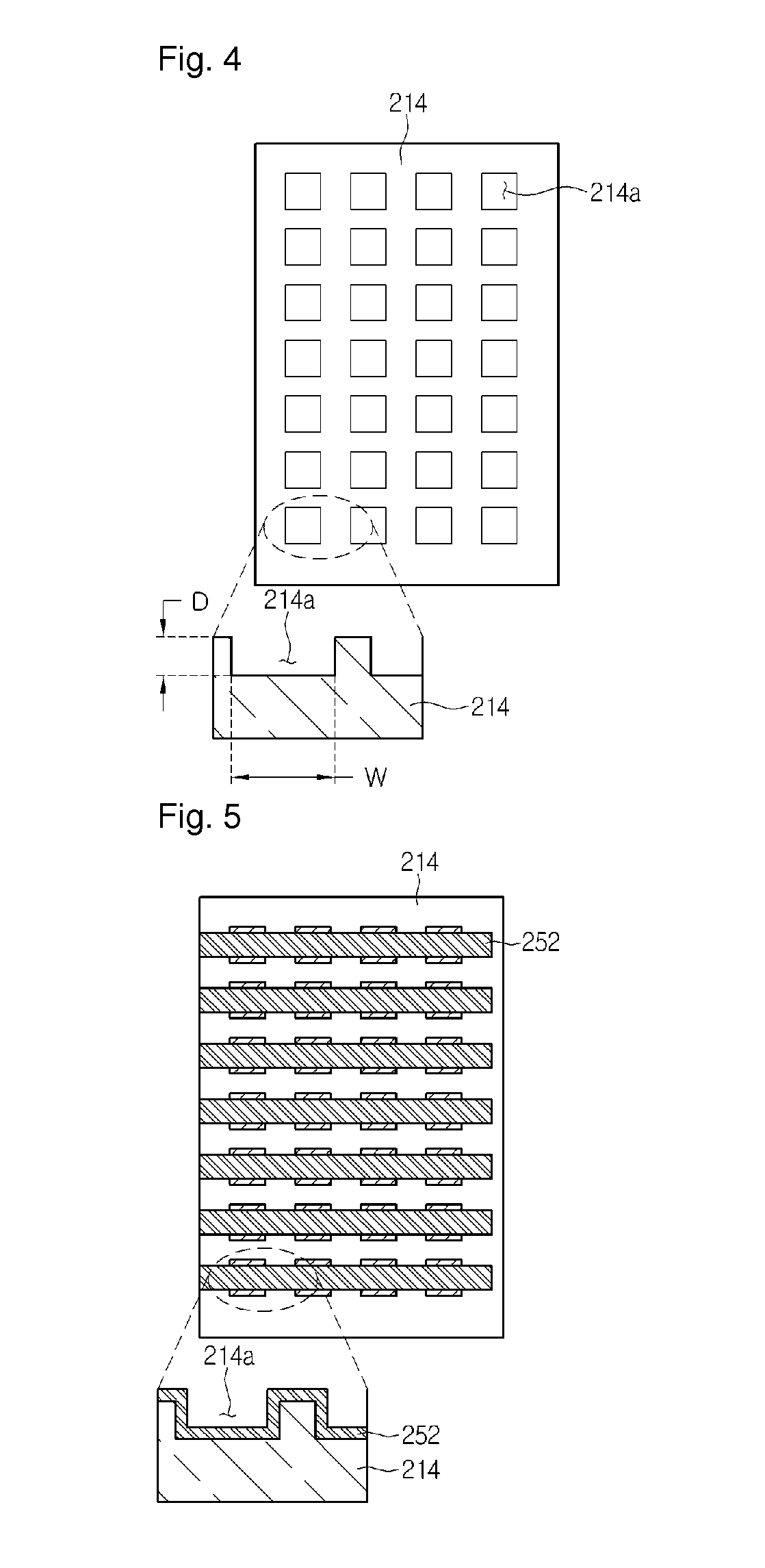
[0031]First, a touch panel will be described in detail with reference to FIGS. 1 to 8.
[0032]FIG. 1 is a schematic plan view showing the touch panel according to the first embodiment, FIG. 2 is a sectional view taken along line A-A′ of FIG. 1, FIG. 3 is an enlarged plan view of a ‘B’ portion of an input unit included in the touch panel according to the first embodiment shown in FIG. 1, and FIGS. 4 to 8 are plan views for explaining the manufacturing process of a haptic unit included in the touch panel according to the first embodiment.
[0033]Referring to FIGS. 1 to 8, the touch panel according to the first embodiment includes an active area AA for detecting apposition of an input device and a dummy area DA disposed around the active area AA.
[0034]A transparent electrode 130 for detecting the input device may be formed on the active area AA. In addition, a wiring 140 connected to the transparent electrode 130 and a printed circuit board connecting the wiring 140 to an external circuit...
second embodiment
[0084]FIG. 9 is a sectional view showing the touch panel according to the
[0085]Referring to FIG. 9, the touch panel according to the second embodiment has no the first substrate 112 (see, FIG. 2) provided in the touch panel according to the first embodiment. That is, the input unit and the haptic unit are provided on the same substrate. In detail, the substrate includes a first surface and a second surface opposite to each other, the input unit is provided on the first surface, the haptic unit is provided on the second surface. According to the transparent electrode 130, the wiring 140, the recess part 214a, the actuator 260 and the electrode units 252 and 254 are formed on the second substrate 214, so the thickness of the touch panel may be reduced.
third embodiment
[0086]Hereinafter, a touch panel will be described with reference to FIG. 10.
[0087]FIG. 10 is a sectional view showing the touch panel according to the third embodiment.
[0088]Referring to FIG. 10, the touch panel according to the third embodiment has a structure in which the haptic unit 200 is turned over as compared with the haptic unit 200 of the touch panel according to the first embodiment. In detail, the recess part 214a is formed on the bottom surface of the second substrate 214 so that the actuator 260 positioned in the recess part 214a may be more stably protected from the external impact and contamination.
[0089]Hereinafter, a liquid crystal display (LCD) according to the embodiment will be described with reference to FIG. 11. FIG. 11 is a schematic sectional view showing the LCD according to the embodiment.
[0090]The LCD according to the present embodiment may include a liquid crystal panel in which the touch panel according to the first embodiment is mounted. The touch pan...
PUM
| Property | Measurement | Unit |
|---|---|---|
| depth | aaaaa | aaaaa |
| width | aaaaa | aaaaa |
| thickness | aaaaa | aaaaa |
Abstract
Description
Claims
Application Information
 - R&D
- Intellectual Property
- Life Sciences
- Materials
- Tech Scout
- Unparalleled Data Quality
- Higher Quality Content
- 60% Fewer Hallucinations
Browse by: Latest US Patents, China's latest patents, Technical Efficacy Thesaurus, Application Domain, Technology Topic, Popular Technical Reports.
© 2025 PatSnap. All rights reserved.Legal|Privacy policy|Modern Slavery Act Transparency Statement|Sitemap|About US| Contact US: help@patsnap.com


