
Methods for bonding substrates

a technology of substrates and adhesives, applied in the direction of sleeve/socket joints, mechanical equipment, transportation and packaging, etc., can solve the problems of incomplete curing of adhesives, difficulty or inability to provide adequate moisture, cost-effective yield and productivity loss, etc., to improve the performance and performance of assemblies, improve the effect of fabrication, performance and refurbishmen

Active Publication Date: 2017-04-18
APPLIED MATERIALS INC
View PDF8 Cites 4 Cited by
  • Summary
  • Abstract
  • Description
  • Claims
  • Application Information

AI Technical Summary

Benefits of technology

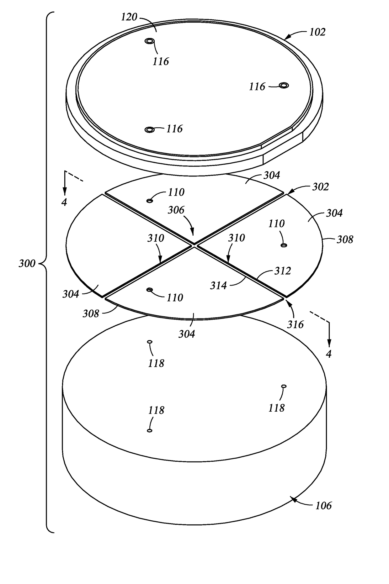
The patent describes methods for bonding substrates (such as an electrostatic puck to a temperature control base) using an adhesive that has been segmented into multiple parts to improve fabrication, performance, and refurbishment of the assembly. These segments have a channel between them, which makes it easy to debond the substrates for refurbishment. The channel also allows for outgassing of volatiles between the substrates, ensuring a uniform temperature profile and heat transfer performance over the life of the assembly.

Problems solved by technology

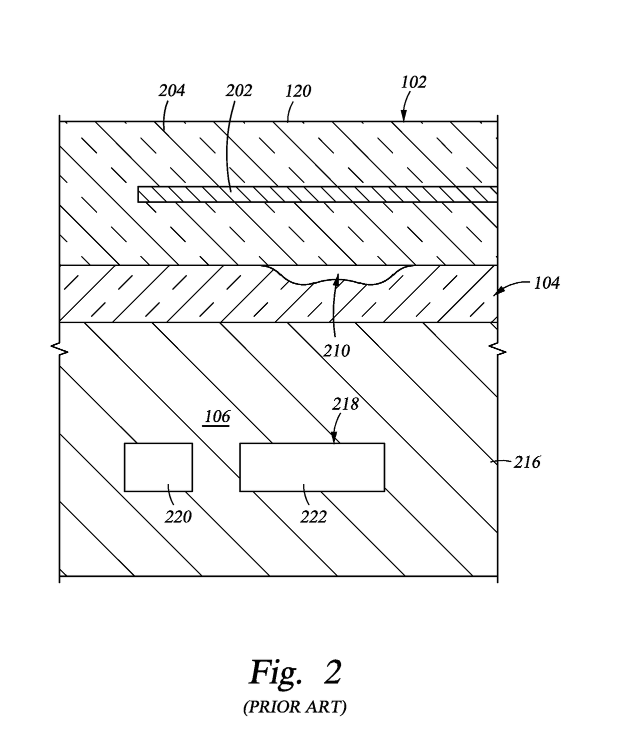
The void 210 increases thermal impedance between the electrostatic puck 102 and the temperature control base 106 which can result in out-of-spec temperature uniformity on the substrate (e.g., wafer) processed, which in turn leads to costly loss of yield and productivity.
Adequate moisture availability becomes difficult or impossible when the adhesive layer is very thin relative to the diameter of the adhesive layer resulting in incomplete curing of the adhesive.
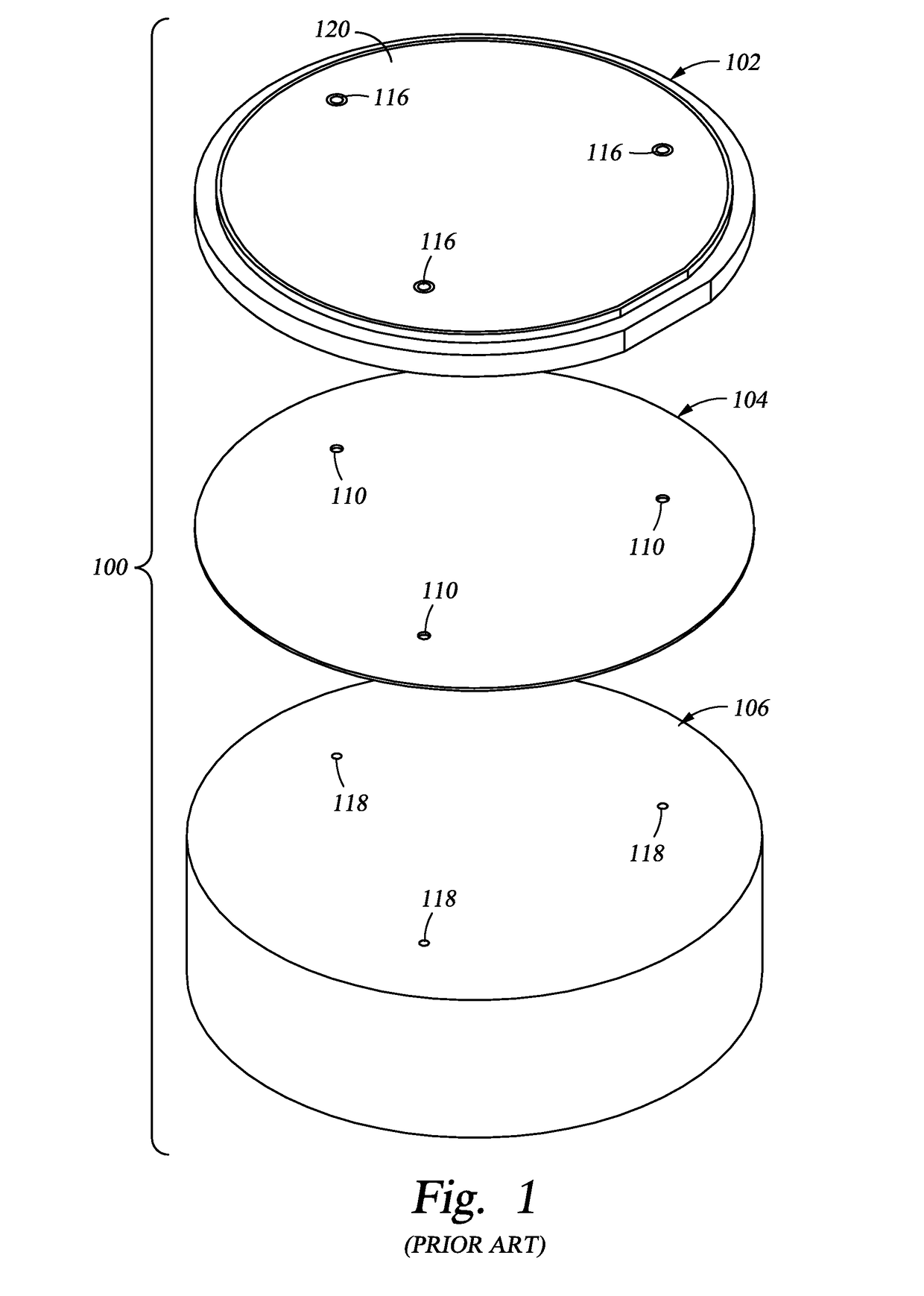
Thus, refurbishment of conventional electrostatic chuck assemblies 100 may be labor intensive, have high scrap rates and be undesirably expensive.
The above mentioned problems are not unique to electrostatic chuck assemblies, but present to some extent in just about all semiconductor chamber components which utilize a contiguous layer of adhesive to bond two substrates.
This problem also exists in display and solar vacuum processing applications as well where the bonding surface areas can be much larger.

Method used


Image

  • Methods for bonding substrates
  • Methods for bonding substrates
  • Methods for bonding substrates

Examples


Embodiment Construction

[0035]Embodiments of the invention generally provide a method for bonding substrates, assemblies fabricated by the same, along with improved methods for refurbishing said assemblies. Embodiments of the invention described herein take advantage of at least one channel partially bounded by an adhesive utilized to join two substrates. In certain embodiments of the invention, the channel is defined between adjacent segments of an adhesive layer bonding the substrates together. The channel is open to an exterior of the substrate assembly, thus providing a vent path for volatile gases outgassed from the adhesive layer to escape from between the substrates, either during curing or use of the assembly. Advantageously, the vent path enhances better curing of the adhesive layer. The vent path also prevents gas pockets from forming between the substrates which could adversely affect the temperature profile across the surface of the substrates. By improving reliability of the ability to control...


PUM

PropertyMeasurementUnit
thicknessaaaaaaaaaa
tensile strengthaaaaaaaaaa
diameteraaaaaaaaaa

Abstract

Methods for bonding substrates, forming assemblies using the same, along with improved methods for refurbishing said assemblies are disclosed that take advantage of at least one channel formed in an adhesive utilized to join two substrates to improve fabrication, performance and refurbishment of the assemblies. In one embodiment an assembly includes a first substrate secured to a second substrate by an adhesive layer. The assembly includes a channel having at least one side bounded by the adhesive layer and having an outlet exposed to an exterior of the assembly.

Description

CROSS-REFERENCE TO RELATED APPLICATIONS[0001]This application claims benefit of U.S. Provisional Application Ser. No. 61 / 703,220, filed Sep. 19, 2012, of which is incorporated by reference in its entirety.BACKGROUND OF THE INVENTION[0002]Field of the Invention[0003]Embodiments of the present invention generally relate to a method for bonding substrates and components suitable for use in a semiconductor processing chamber fabricated by the same, using a segmented bond design.[0004]Description of the Related Art[0005]In substrate processing applications, many chamber parts and components are fabricated using two or more parts, or substrates, bonded together. Examples of such components includes electrostatic pucks bonded to temperature control supports, showerheads bonded to gas distribution plates, and heaters bonded to chamber lids, among others.[0006]FIG. 1 is an example of a conventional chamber part comprising substrates bonded together illustrated as an electrostatic chuck assem...

Claims


Application Information

Patent Timeline
Patent Type & Authority Patents(United States)
IPC IPC(8): B32B7/12H01L21/67B32B3/20B32B7/14H01L21/687H01L21/683
CPCH01L21/67005B32B7/14H01L21/67092H01L21/6831H01L21/6833H01L21/6835H01L21/68785H01L21/67109H01L2221/68318H01L2221/68381H01L2224/2732H01L2224/27318H01L2224/27436H01L2224/27438H01L2224/29011H01L2224/29012H01L2224/29013H01L2224/29014H01L2224/2919H01L2224/29078H01L2224/29191H01L2224/83862H01L2224/83877H01L2224/98H01L2924/15151Y10T156/10Y10T279/23Y10T428/24851H01L2924/00012H01L2924/00014H01L21/02008H01L21/02109H01L21/02299H01L21/20B32B37/1292
Inventor NARENDRNATH, KADTHALA RAMAYASHEELAVANT, GANGADHARAGARWAL, MONIKABHATNAGAR, ASHISH
Owner APPLIED MATERIALS INC
Learn More