Imaging device and electronic device
a technology of electronic devices and imaging devices, applied in the direction of radio-controlled devices, television system scanning details, television systems, etc., can solve the problems of difficult to reduce the variation in electrical characteristics, long total imaging time, and increase the difficulty of transistor manufacturing process, etc., to achieve high sensitivity, wide dynamic range, and high quality imaging data
- Summary
- Abstract
- Description
- Claims
- Application Information
AI Technical Summary
Benefits of technology
Problems solved by technology
Method used
Image
Examples
embodiment 1
[0083]In this embodiment, an imaging device that is one embodiment of the present invention is described with reference to drawings.
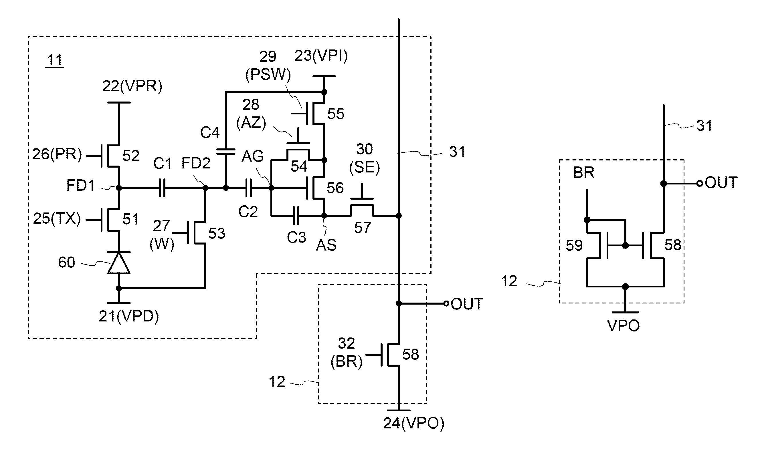
[0084]An imaging device in one embodiment of the present invention includes a pixel circuit that can compensate variation in threshold voltage of a source follower amplifier transistor in a pixel of an imaging device that outputs signal charge (data) by a source follower.
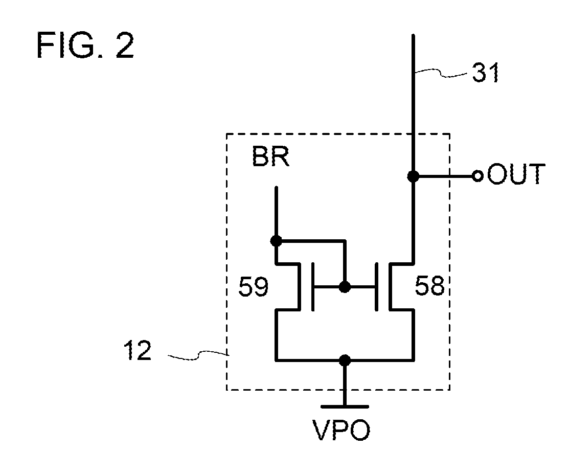
[0085]FIG. 1 is a circuit diagram of a circuit 11 that can function as a pixel circuit and a circuit 12 that can function as a reference current source circuit included in an imaging device in one embodiment of the present invention. In FIG. 1 and the like, transistors are n-ch transistors; however, one embodiment of the present invention is not limited thereto. The transistors may be p-ch transistors by reversing the magnitude relationship of a potential as illustrated in FIG. 47. Alternatively, some of the n-ch transistors may be replaced with p-ch transistors.
[0086]The circuit 11 is ...
embodiment 2
[0167]In this embodiment, an example of a method for driving a pixel circuit is described.
[0168]The pixel circuit described in Embodiment 1 can perform first operation in which normal imaging is performed and second operation in which differential data of imaging data of an initial frame and imaging data of a current frame can be retained and a signal based on the differential data can be output. In the second operation, differential data can be output without a comparison process or the like in an external circuit; thus, the pixel circuit can be applied to a low-power security camera or the like.
[0169]As illustrated in FIGS. 17A and 17B, an imaging device in one embodiment of the present invention includes a pixel portion 400 that includes the circuits 11 arranged in a matrix, a row driver 410 connected to the circuits 11, the circuits 12 connected to the circuits 11, an A / D converter 420 connected to the circuits 12, and a column driver 430 connected to the A / D converter 420. The ...
embodiment 3
[0186]In this embodiment, an example of a method for driving a pixel circuit is described.
[0187]As described in Embodiment 2, the operation of the pixel circuit is repetition of the reset operation, the accumulation operation, and the selection operation. As imaging modes in which the whole pixel matrix is controlled, a global shutter system and a rolling shutter system are known.
[0188]FIG. 20A is a timing chart of a global shutter system. The timing chart illustrates operation of an imaging device in which a plurality of pixel circuits in FIG. 1 are arranged in a matrix. Specifically, the timing chart illustrates operation of the pixel circuits from a first row to an n-th row (n is a natural number of 3 or more). The operation is described giving the first operation described in Embodiment 2 as an example.
[0189]In FIG. 20A, a signal 501, a signal 502, and a signal 503 are input to the wirings 26 (PR) connected to the pixel circuits in the first row, the second row, and the n-th row...
PUM
 Abstract
Description
Claims
Application Information
 - R&D
- Intellectual Property
- Life Sciences
- Materials
- Tech Scout
- Unparalleled Data Quality
- Higher Quality Content
- 60% Fewer Hallucinations
Browse by: Latest US Patents, China's latest patents, Technical Efficacy Thesaurus, Application Domain, Technology Topic, Popular Technical Reports.
© 2025 PatSnap. All rights reserved.Legal|Privacy policy|Modern Slavery Act Transparency Statement|Sitemap|About US| Contact US: help@patsnap.com


