Neuromorphic device with excitatory and inhibitory functionalities

a neuromorphic device and functional technology, applied in semiconductor devices, digital storage, instruments, etc., can solve the problems of large increase in power consumption, large increase in complexity of interconnection for excitatory or inhibitory functions, and high cost, so as to reduce the area of neuromorphic devices, reduce power consumption, and efficiently use

Active Publication Date: 2016-08-30
SEOUL NAT UNIV R&DB FOUND
View PDF4 Cites 21 Cited by
  • Summary
  • Abstract
  • Description
  • Claims
  • Application Information

AI Technical Summary

Benefits of technology

[0016]The present invention is to provide a neuromorphic device capable of having excellent reliability, lower power consumption, and a high degree of integration while solving problems of existing neuromorphic devices.
[0022]In the neuromorphic device array according to the second aspect, preferably, each of the first and second lower insulating film stacks of each neuromorphic device of the neuromorphic device array includes a charge storage layer, and in the case of selectively storing positive or negative charges in the charge storage layers of the first and second lower insulating film stacks of a specified neuromorphic device, a voltage is applied to the upper electrodes of the other neuromorphic devices, so that storing charges in the other neuromorphic devices is negligible.
[0024]A neuromorphic device according to the present invention is configured to include two MOS transistors including a common source and to read information stored in a charge storage layer enabling a memory function, so that the neuromorphic device can imitate an excitation transmitting function of neurons and synapses. In addition, the neuromorphic device according to the present invention is configured with two elements, so that the area of the neuromorphic device can be reduced.
[0025]In addition, the two MOSFETs included in one neuromorphic device in order to imitate one synapse are controlled to have different threshold voltages in a positive or negative region, and thus, when an input voltage to the neuromorphic device is 0 V (or the synapse is not operated), no current flows, so that power consumption can be reduced.
[0026]In addition, the neuromorphic device configured to include two MOSFETs can be controlled to have an excitatory or inhibitory functionality in a reconfigurable manner, so that the area of the neuromorphic device can be efficiently used. In addition the neuromorphic device according to the present invention can implement a spike timing dependent plasticity (STDP) function, a short term plasticity (STP) function, and long term plasticity (LTP) function as well as a memory function while occupying a small area. In addition, functions of a biological synapse are imitated on the basis of semiconductor FETs, and thus, selection elements causing problems in existing memrister-based techniques can be removed, so that durability and reliability can be greatly improved.
[0027]In comparison with existing neuromorphic devices, according to the present invention, it is possible to provide a neuromorphic device capable of imitating functions of neurons and synapses such as an excitation transmitting function, an excitation integrating / transmitting function, and excitatory and inhibitory functionalities and having excellent durability and a high degree of integration.

Problems solved by technology

Recently, in integrated circuits based on a Von Neumann architecture, power consumption has been greatly increased, and the problem of heat release has been very serious.
However, in implementation of an actual synapse array, complexity of interconnection for the excitatory or inhibitory functionality is greatly increased.
In addition, there is a problem in that, as a limitation of the two-terminal element in an array environment, a selection element needs to be installed in each neuromorphic device.
However, in the case of using the SRAM, since the SRAM is a digital memory, there is a limitation to implement one synapse.
In particular, the case of using the RRAM has a serious problem in durability, and the case of using the PRAM has a problem in durability and a problem according to high power consumption.
Since an existing SRAM cell for imitating the synapse is typically configured with eight transistors, the occupied area is too large, and there is a limitation as a digital memory described above.
Therefore, there is a serious problem in degree of integration.

Method used


Image

  • Neuromorphic device with excitatory and inhibitory functionalities
  • Neuromorphic device with excitatory and inhibitory functionalities
  • Neuromorphic device with excitatory and inhibitory functionalities

Examples


first embodiment

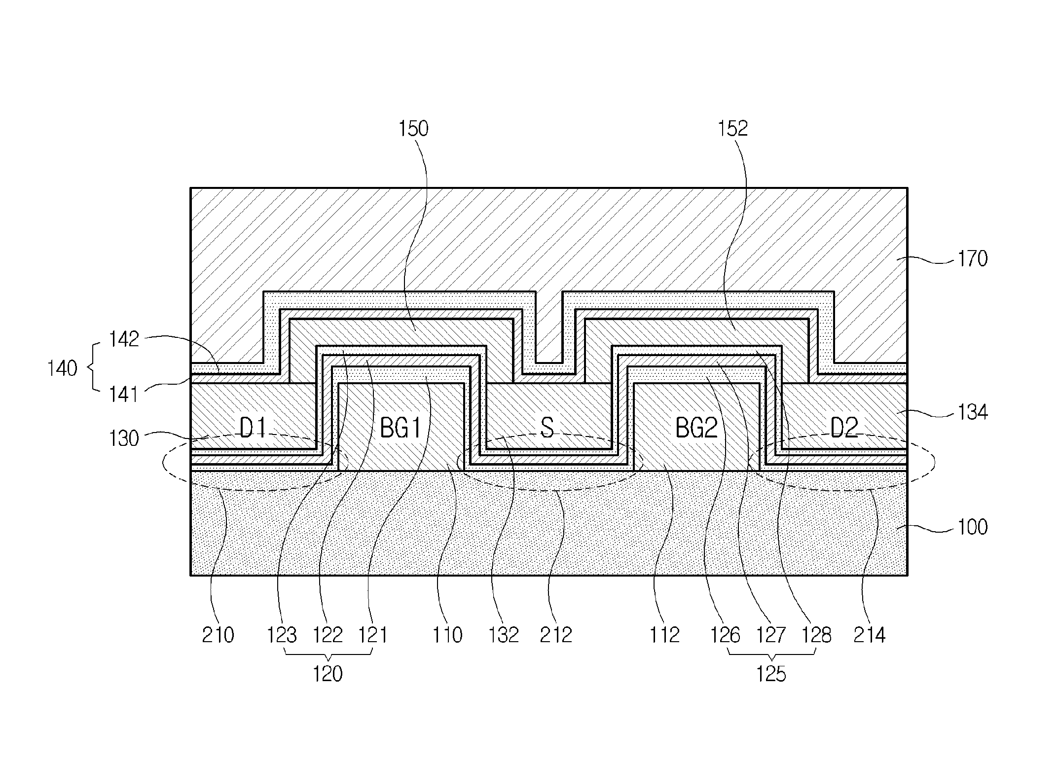
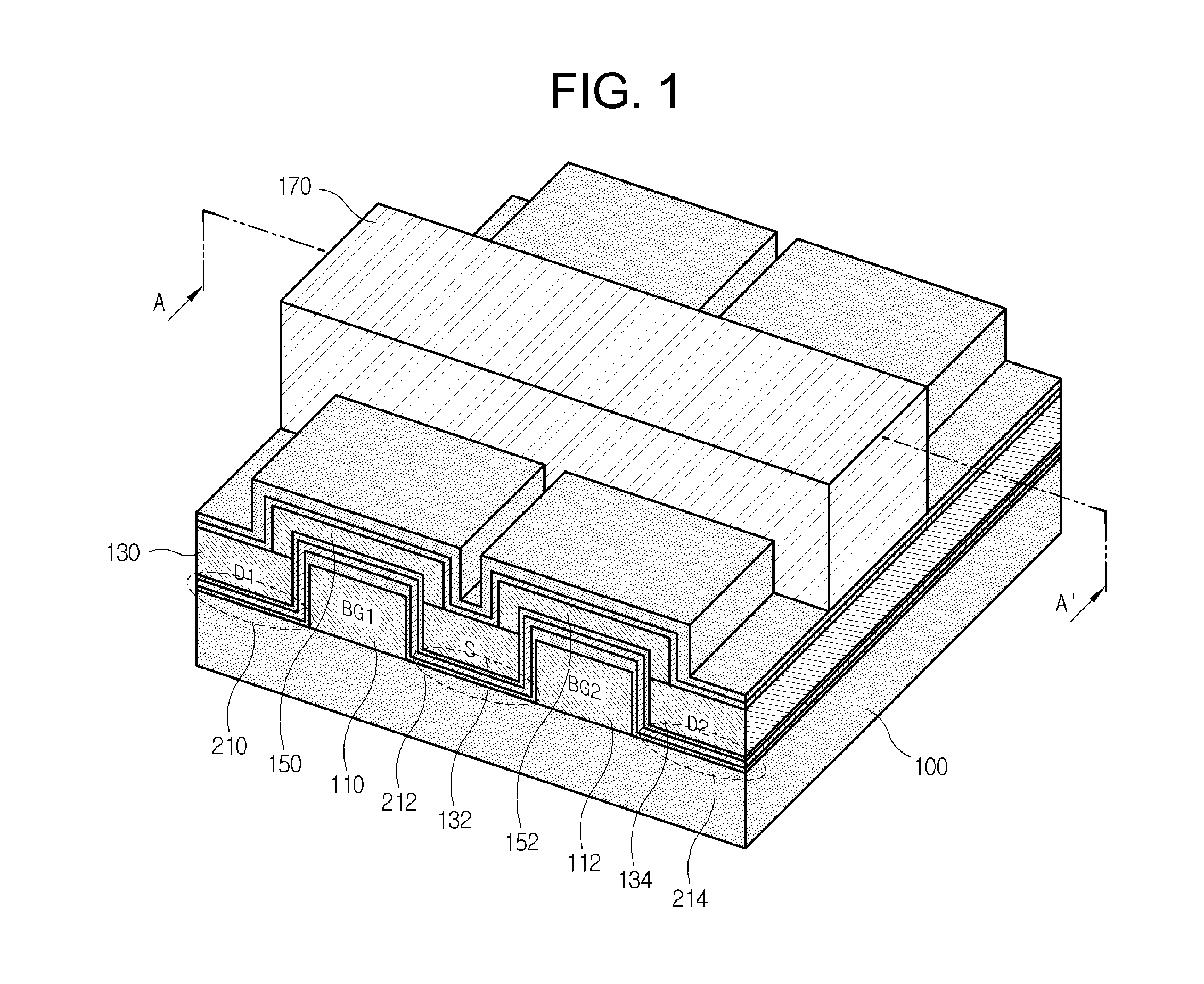
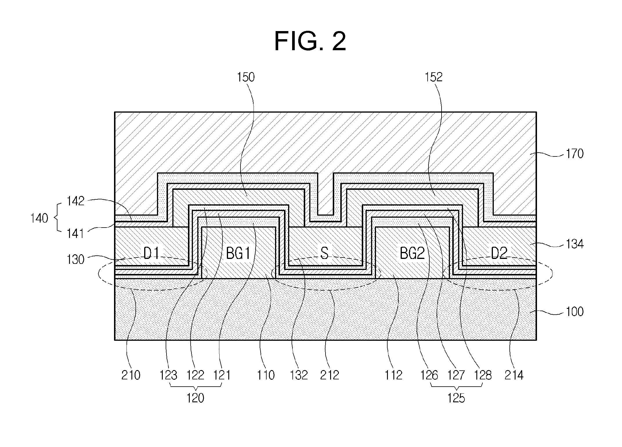
[0049]FIG. 1 is a perspective diagram illustrating a neuromorphic device according to the present invention. FIG. 2 is a cross-sectional diagram taken along line A-A′ of FIG. 1.

[0050]Referring to FIGS. 1 to 2, the neuromorphic device 10 according to the embodiment is configured to include a substrate 100, first and second lower electrodes (BG1 and BG2) 110 and 112 which are formed on the substrate to be electrically isolated from each other, a first lower insulating film stack 120 which is formed on a top surface and sidewalls of the first lower electrode, a second lower insulating film stack 125 which is formed on a top surface and sidewalls of the second lower electrode, a first, second, and third doped regions 130, 132, and 134 which are formed at the left and right of the first and second lower electrode, first and second semiconductor regions 150 and 152 which are formed on the first and second lower insulating film stacks, an upper insulating film stack 140 which is formed on ...

second embodiment

[0066]FIG. 3 is a perspective diagram illustrating a neuromorphic device according to the present invention. FIG. 4 is a cross-sectional diagram taken along line B-B′ of FIG. 3.

[0067]Referring to FIGS. 3 and 4, the neuromorphic device according to the second embodiment has a structure similar to that of the neuromorphic device according to the first embodiment except that lower insulating film stacks are not formed between the first doped region and the substrate, between the second doped region and the substrate, and between the third doped region and the substrate. Therefore, the first doped region 130, the second doped region 132, and the third doped region 134 are formed directly on the substrate 100.

[0068]In the above-described neuromorphic devices according to the first and second embodiments, programming and erasing can be performed element by element by using the first and second lower electrodes and the upper electrode. In the neuromorphic device according to the present in...


PUM


Abstract

Provided is a neuromorphic device including first and second lower electrodes formed on a substrate to be electrically separated, first and second lower insulating film stacks formed at least on respective surfaces of the first and second lower electrodes, first, second, and third doped regions formed at left and right sides of the first and second lower electrodes, first and second semiconductor regions formed on the first and second lower insulating film stacks, an upper insulating film stack formed on the first and second semiconductor regions and the first, second, and third doped regions, and an upper electrode formed on the upper insulating film stack. Accordingly, a specified neuromorphic device can be reconfigured to have arbitrarily inhibitory or excitatory functionality by using the first and second lower electrodes and the lower insulating film stacks including charge storage layers formed on the surfaces of the electrodes.

Description

FUNDING STATEMENT[0001]This invention was supported by Samsung Research Funding Center of Samsung Electronics under Project Number SRFC-IT1301-08.BACKGROUND OF THE INVENTION[0002]1. Field of the Invention[0003]The present invention relates to a neuromorphic device imitating a synapse, a synapse array, or a neuron in a neuromorphic technique.[0004]2. Description of the Related Art[0005]Recently, in integrated circuits based on a Von Neumann architecture, power consumption has been greatly increased, and the problem of heat release has been very serious. Therefore, in the field of Von-Neumann-based integrated circuits, many approaches to imitate nervous systems of animals have been studied. In particular, in techniques of imitating the nervous systems of animals, the power consumption can be greatly reduced, and perceiving and learning are enabled, so that perception and determination functions can be improved. Accordingly, the functions of existing Von-Neumann-based integrated circui...

Claims


Application Information

Patent Timeline
Patent Type & Authority Patents(United States)
IPC IPC(8): H01L29/76G11C11/54H01L29/417H01L29/08H01L27/115
CPCG11C11/54H01L27/11521H01L27/11568H01L29/0847H01L29/41758H01L29/4234H01L29/792H01L29/41733H01L29/78696H10B43/30H10B41/30
Inventor LEE, JONG-HOKIM, CHUL-HEUNGWOO, SUNG-YUN
Owner SEOUL NAT UNIV R&DB FOUND
Why Eureka
Try Eureka