Liquid crystal display device and mother substrate

a display device and liquid crystal technology, applied in non-linear optics, instruments, optics, etc., can solve the problems of difficult to maintain the distance between the tft substrate and the counter substrate constant, complicated process, and loss of scan line driving circuit, so as to prevent uneven gap of liquid crystal display, and prevent uneven brightness and color

Active Publication Date: 2016-04-19
JAPAN DISPLAY INC
View PDF13 Cites 5 Cited by
  • Summary
  • Abstract
  • Description
  • Claims
  • Application Information

AI Technical Summary

Benefits of technology

[0009]In the display device, for example, in the liquid crystal display device, a driving circuit is directly formed into the liquid crystal display panel in order to reduce the overall size of the liquid crystal display device and reduce the number of leaders of lines. In this case, when the driving circuit is formed by poly silicon, the circuit characteristics are improved. However, when the TFT in the pixel area is formed by a-Si, the process is complicated. On the other hand, the circuit size of the scan line driving circuit is smaller than that of the image signal line driving circuit, so that the scan line driving circuit can be formed by a-Si. For this reason, only the scan line driving circuit is directly formed by a-Si into the liquid crystal display panel and the image signal line driving circuit is formed by an IC driver. In such a structure, if the glass fiber is used for gap adjustment in the sealing portion, there is a risk that the scan line driving circuit will be destroyed. Thus, it is necessary to use the cylindrical spacer formed by a resin.
[0011]It would be desirable to provide a liquid crystal display device in which the distance between the TFT substrate and the counter substrate does not vary, so that uneven brightness, uneven color, or other imperfections are not likely to occur in the liquid crystal display panel without using the inorganic passivation film that serves as a flattening film.
[0014]According to the present invention, it is possible to equalize the distance between the TFT substrate and the counter substrate in the liquid crystal display panel. Thus, it is possible to prevent uneven gap of the liquid crystal display. In other words, it is possible to prevent uneven brightness and color due to the variation of the distance between the TFT substrate and the counter substrate. The mount, which is a feature of the present invention, can be formed when the display area of the liquid crystal display panel is formed. Thus, the number of steps of the manufacturing process is not increased. As a result, it is possible to prevent the uneven brightness and color in the liquid crystal display device without an increase in the production cost.

Problems solved by technology

However, when the TFT in the pixel area is formed by a-Si, the process is complicated.
In such a structure, if the glass fiber is used for gap adjustment in the sealing portion, there is a risk that the scan line driving circuit will be destroyed.
In this case, even if the cylindrical spacer is used, it is difficult to maintain the distance between the TFT substrate and the counter substrate to be constant.

Method used


Image

  • Liquid crystal display device and mother substrate
  • Liquid crystal display device and mother substrate
  • Liquid crystal display device and mother substrate

Examples


first embodiment

[0028]FIG. 1 is a plan view of a TFT substrate 100 according to the present invention. In FIG. 1, scan lines 10 extend in the horizontal direction and are arranged in the vertical direction in the display area. A scan line driving circuit 12 is formed on the left side of the TFT substrate 100. The scan lines 10 extend in the horizontal direction from the scan line driving circuit 12. Scan line driving circuit leaders 11 are formed in the scan line driving circuit to fetch signals from the outside. In FIG. 1, image signal lines 20 extend in the vertical direction and are arranged in the horizontal direction. Then, image signal line leaders 21 extend from the image signal lines 20 to an IC driver 40.

[0029]The peripheral area between the dashed lines and the end portion shown in FIG. 1 is a sealing portion 50. In FIG. 1, a mount 140 for a cylindrical spacer 150 formed in a counter substrate 200, not shown, is formed in the area where the lines are not present. In FIG. 1, this correspon...

second embodiment

[0041]In order to increase the productivity of liquid crystal display panels, a large number of liquid crystal display panels (liquid crystal cells) are formed in a mother substrate 1000 to simultaneously form a large number of liquid crystal cells. Thus, if the distance between the TFT substrate 100 and the counter substrate 200 in each liquid crystal cell is not properly provided in the state of the mother substrate 1000, this will appear as uneven gap of the product.

[0042]FIG. 7 is a schematic plan view of the structure to solve this problem. FIG. 7 shows the mother substrate 1000 in which a large number of liquid crystal cells are formed. The mother substrate 1000 is formed by bonding a mother TFT substrate in which a large number of TFT substrates 100 are formed, and a mother counter substrate in which a large number of counter substrates 200 are formed, by a mother substrate sealing material 500 as well as the sealing material 50 formed in each liquid crystal display panel.

[00...

third embodiment

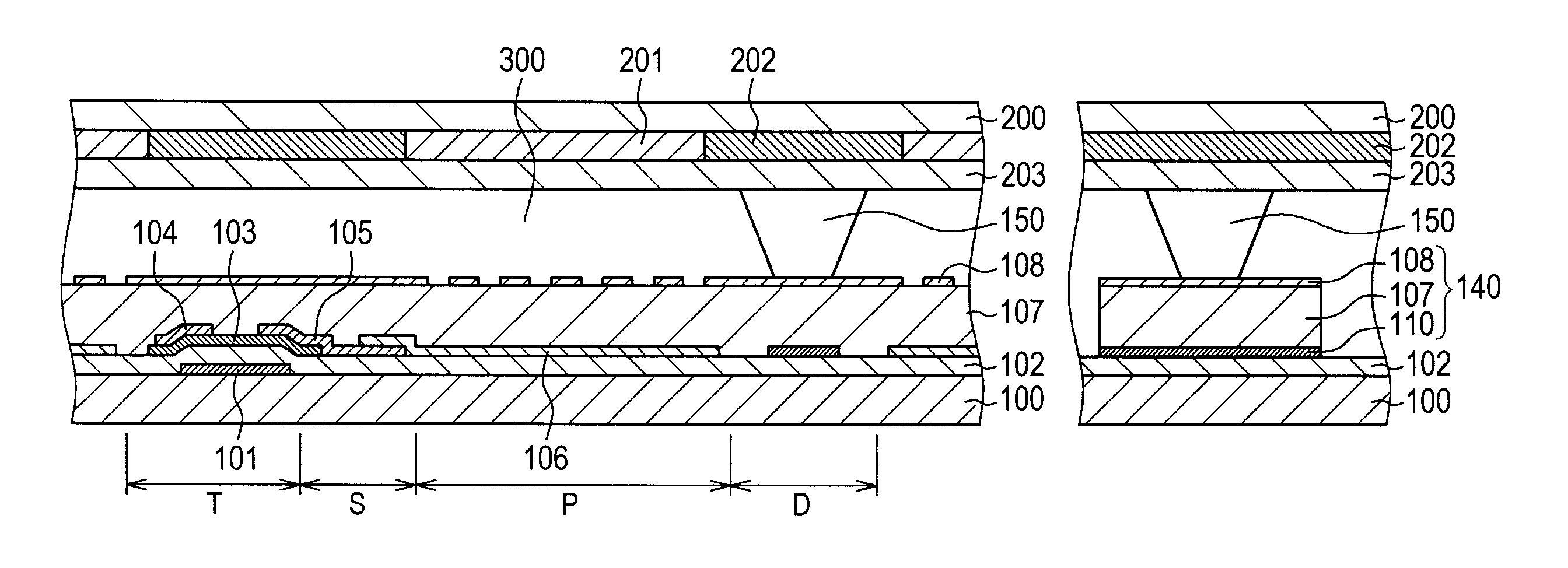
[0050]A third embodiment is an example in which the cylindrical spacer 150 is formed on the TFT to maintain the distance between the TFT substrate 100 and the counter substrate 200 in the display area. In FIG. 11, in the display area, the cylindrical spacer 150 formed in the counter substrate 200 comes into contact above the TFT formed in the TFT substrate 100. In this case, the structure of the mount 140 within the sealing portion 50 shown in FIG. 1, has the gate electrode 101, the gate insulating film 102, the a-Si film 103, the source-drain layer 105, the inorganic passivation film 107, and the ITO forming the common electrode 108, in this order from the bottom in the counter substrate 200. Thus, the mount 140 shown in the right side of FIG. 11 has the same layer structure as that of the mount 140 shown in FIG. 1. Here, in the mount 140 shown in the right side of FIG. 11, the gate electrode 101, the source-drain electrode 105, and the ITO 108 are conductive films. These conductiv...


PUM

PropertyMeasurementUnit
areaaaaaaaaaaa
brightnessaaaaaaaaaa
coloraaaaaaaaaa

Abstract

In a liquid crystal display device including a TFT substrate and a counter substrate, when an organic passivation film is not formed in the TFT substrate, the distance between the TFT substrate and the counter substrate in the display area of a liquid crystal display panel is provided by a cylindrical spacer. Also, the distance in the area where pixels, scan lines, and image signal lines are not formed within the liquid crystal display panel is provided by the cylindrical spacer. In this case, it is necessary to form a mount. The layer structure of the mount is the same as that of the TFT substrate with which the cylindrical spacer in the display area comes into contact. This makes it possible to equalize the distance of the liquid crystal layer of the liquid crystal display panel without an increase in production cost, and to prevent uneven brightness or color.

Description

CLAIM OF PRIORITY[0001]The present application claims priority from Japanese Patent Application JP 2011-131714 filed on Jun. 14, 2011, the content of which is hereby incorporated by reference into this application.FIELD OF THE INVENTION[0002]The present invention relates to a display device, and more particularly to a display device that can equalize the distance between upper and lower substrates to prevent the degradation of the display quality such as uneven brightness and color.BACKGROUND OF THE INVENTION[0003]A display device, for example, a liquid crystal display panel used for a liquid crystal display device, includes a TFT substrate, a counter substrate facing the TFT substrate, and a liquid crystal sandwiched between the TFT substrate and the counter substrate. In the TFT substrate, pixels having pixel electrodes, thin film transistors (TFT) and the like are arranged in a matrix. In the counter substrate, color filters and the like are formed at locations corresponding to t...

Claims


Application Information

Patent Timeline
Patent Type & Authority Patents(United States)
IPC IPC(8): G02F1/1339G02F1/1333
CPCG02F1/133345G02F1/13394G02F1/133351G02F2001/133357G02F1/133357G02F1/133512G02F1/133514
Inventor NAGAMI, TAKAHIRO
Owner JAPAN DISPLAY INC
Why Eureka
Try Eureka