
Substrate structure and manufacturing method thereof

a technology of substrate structure and manufacturing method, which is applied in the direction of lithographic mask, laminating printed circuit board, semiconductor/solid-state device details, etc., can solve the problems of difficult to reduce the thickness of the package structure, and achieve the effect of saving manufacturing time, improving production efficiency, and easy removal

Active Publication Date: 2016-04-12
SUBTRON TECH
View PDF5 Cites 0 Cited by
  • Summary
  • Abstract
  • Description
  • Claims
  • Application Information

AI Technical Summary

Benefits of technology

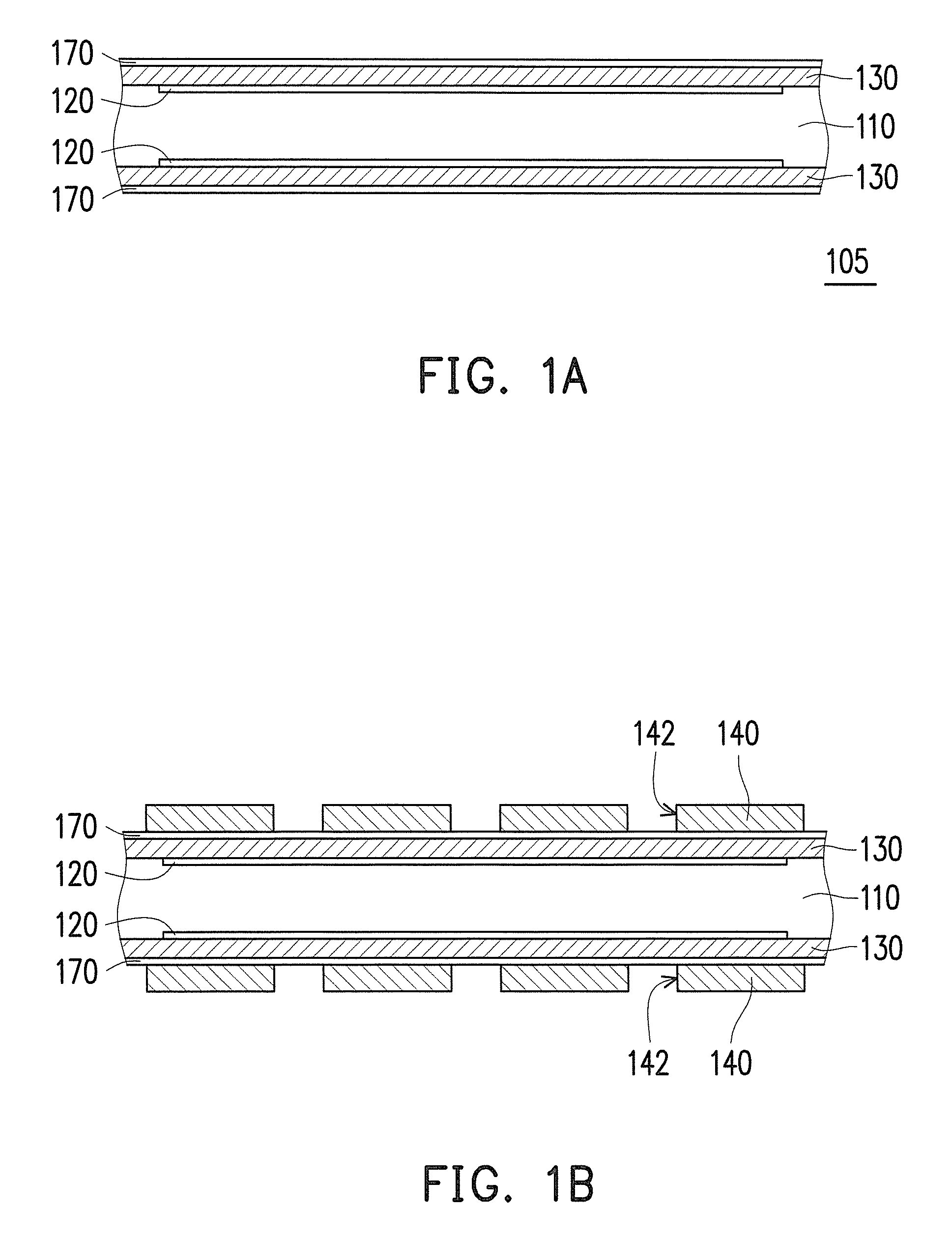
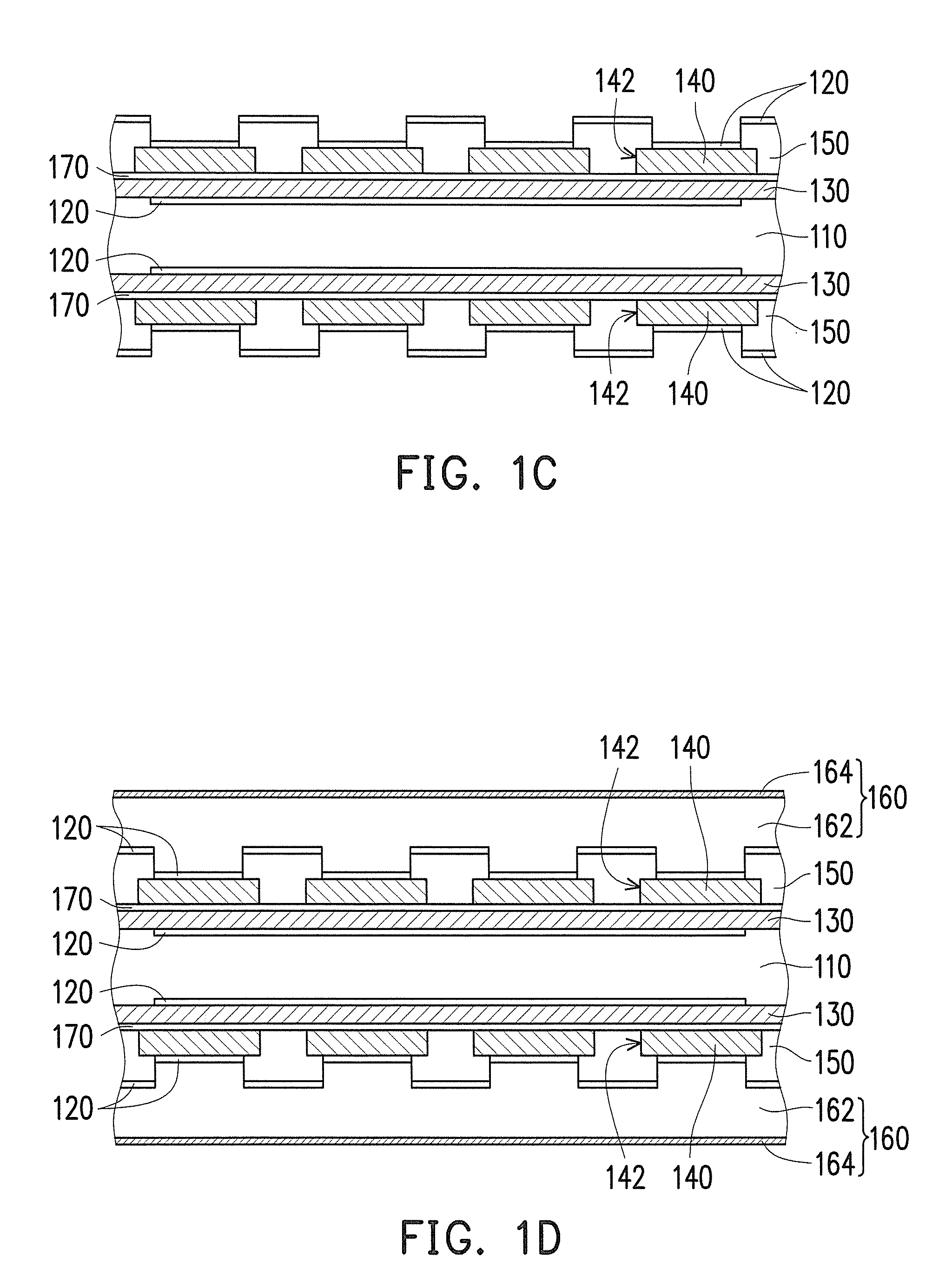
[0013]Based on the above, for the substrate structure of the invention, the manufacturing processes of the substrate structure are respectively performed on a separable substrate in a symmetrical manner. Accordingly, after a substrate separation is performed, two substrate structures independent from each other may be obtained, so as to effectively save the manufacturing time and improve the production efficiency. In addition, in the separable substrate of the invention, the release layer is connected between the supporting layer and the patterned metal layer of the substrate, such that after the stacking layer is formed, the supporting layer can be easily removed by taking advantage of the separability of the release layer. Therefore, compared to a conventional substrate structure which is formed by stacking a plurality of stacking layers on a core layer, the substrate structure of the invention has a smaller overall thickness, and thus a package structure using such substrate structure has a smaller package thickness.

Problems solved by technology

Therefore, if there is a bottleneck in reducing the thickness of the core layer, it will be very difficult to reduce the thickness of the package structure.

Method used


Image

  • Substrate structure and manufacturing method thereof
  • Substrate structure and manufacturing method thereof
  • Substrate structure and manufacturing method thereof

Examples


Embodiment Construction

[0019]The foregoing and other technical contents, features, and effects relating to the invention will be clearly shown in the following detailed description of embodiments with reference to the accompanying drawings. In the following embodiments, wordings used to indicate directions, such as “up,”“down,”“front,”“back,”“left,” and “right”, merely refer to directions in the accompanying drawings. Therefore, the directional wording is used to illustrate rather than limit the invention. In addition, in the following embodiments, the same or like numbers stand for the same or like elements.

[0020]FIGS. 1A to 1G are schematic cross-sectional views illustrating a process of a manufacturing method of a substrate structure according to an embodiment of the invention. The substrate structure of the present embodiment is a single layer structure including a separable substrate. In the present embodiment, the manufacturing method of a substrate structure includes the following steps. First, ref...


PUM

PropertyMeasurementUnit
thicknessaaaaaaaaaa
contact densityaaaaaaaaaa
dielectricaaaaaaaaaa

Abstract

A manufacturing method of a substrate structure includes the following steps. A substrate including a supporting layer, two release layers and two base metal layers is provided. The release layers are disposed on two opposite surfaces of the supporting layer respectively. Each base metal layer covers each of the release layers. A first patterned solder-resist layer is formed on each of the base metal layers. A stacking layer is laminated on each of the base metal layers to cover each of the first patterned solder-resist layers. Each stacking layer includes a dielectric layer and a metal foil. Each dielectric layer is disposed between the corresponding base metal layer and the corresponding metal foil. Each base metal layer is separated from the supporting layer. Each base metal layer is patterned to form a patterned metal layer on each stacking layer. Each patterned metal layer exposes the corresponding first patterned solder-resist layer.

Description

CROSS-REFERENCE TO RELATED APPLICATION[0001]This application claims the priority benefit of Taiwan application serial no. 103115196, filed on Apr. 28, 2014. The entirety of the above-mentioned patent application is hereby incorporated by reference herein and made a part of this specification.BACKGROUND OF THE INVENTION[0002]1. Field of the Invention[0003]The invention relates to a substrate structure and a manufacturing method thereof. More particularly, the invention relates to a substrate structure having a smaller overall thickness and a manufacturing method thereof.[0004]2. Description of Related Art[0005]The purpose of chip packages is to protect exposed chips, to reduce contact density in a chip, and to provide good thermal dissipation for chips. In a common packaging method, the chip is installed onto a package carrier by wire bonding or by flip chip bonding, such that the contacts on the chip may be electrically connected to the package substrate. Therefore, the contacts on ...

Claims


Application Information

Patent Timeline
Patent Type & Authority Patents(United States)
IPC IPC(8): H05K1/02H05K3/14H05K3/00H05K3/06
CPCH05K1/0296H05K3/0058H05K3/06H05K3/14H05K2203/0502H05K2203/0548H05K2203/066H05K3/0061H05K3/048H05K2201/0145H05K2203/0152H05K3/4682H05K1/0298H05K1/09H05K3/064H05K3/4652H01L21/4857H01L21/6835H01L23/13H01L23/49822H01L23/49838H01L23/49866H01L2221/68345H01L2221/68381
Inventor WANG, CHAO-MIN
Owner SUBTRON TECH
Learn More