Memory circuitry including read voltage boost

a memory circuit and read voltage technology, applied in the field of memory circuitry, can solve the problems of reducing the performance of the sense amplifier circuitry, restricting the memory performance, and heavy margin the time required for the sense amplifier, so as to reduce the rate of misreading, improve the performance, and improve the robustness

Active Publication Date: 2016-03-01
RGT UNIV OF MICHIGAN
View PDF4 Cites 0 Cited by
  • Summary
  • Abstract
  • Description
  • Claims
  • Application Information

AI Technical Summary

Benefits of technology

[0014]The present technique uses one or more boost capacitors coupled to the bit lines running through the array of bit cells so as to boost the change in voltage that is supplied to the sense amplifier circuitry for sensing. The increased magnitude of the change in voltage makes it easier for the sense amplifier circuitry to properly sense the data value being read. This boosted voltage may be used to achieve higher performance in terms of read speed, or may be traded for more robustness by using it to decrease the rate of misreads. The technique uses boost control circuitry to connect the boost capacitor or capacitors to the bit line or bit lines in a configuration in which they first sample the initial changing voltage difference occurs. The boost control circuitry then switches to a boost configuration in which the connection of one or more boost capacitors is such that the voltage that they have sampled are added to the voltage change(s) which has occurred on the bit lines so that the change in voltage supplied to the sense amplifier has a greater magnitude making it easier to reliably sense and latch.
[0015]While it will be appreciated that the present techniques may be employed within a wide variety of different types of memory, such as, for example, 8T memory with one bit line for column of bit cells, the present technique may be used in embodiments when the columns of bit lines are coupled to respective bit line pairs and the sense amplifier circuitry is configured to sense of voltage difference between pairs and bit lines. The use of bit line pairs in this way has the advantage of increased resistance to common mode noise arising on the pairs of bit lines.
[0020]In some embodiments the boost control circuitry may be configured to provide a connection between the at least one of the bit lines and the sense amplifier circuitry via a bit line switch (such as a transistor) during the sampling operation and to break this connection during the boost operation. This arrangement facilitates the reconfiguration of the connection between the boost capacitor and the bit line in a manner appropriate to first perform the sampling and then the boosting of the voltage supplied to the sense amplifier circuitry.
[0022]The incorporation of the boost capacitors within the memory may be facilitated when the boost capacitor is provided with a physical pitch dimension which is substantially equal to the pitch dimension of the sense amplifier circuitry excluding that boost capacitor. Accordingly, the provision of the boost capacitor need not impact the density at which the memory may be formed.

Problems solved by technology

A problem within such memory circuits is that as device size has become smaller it is more difficult to match the devices within the sense amplifier circuit resulting in offsets and other mismatches which degrade the performance of the sense amplifier circuitry.
In order to deal with this memory designers typically heavy margin the time required for a sense amplifier to read and latch a bit line voltage.
Such heavy margining restricts the performance of the memory.

Method used


Image

  • Memory circuitry including read voltage boost
  • Memory circuitry including read voltage boost
  • Memory circuitry including read voltage boost

Examples


Embodiment Construction

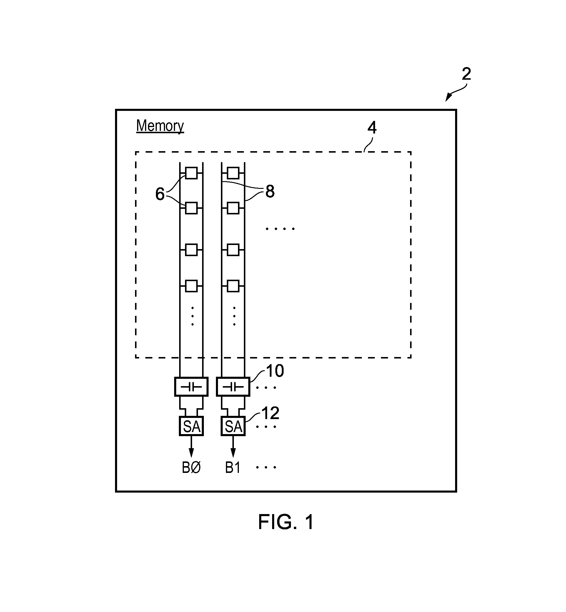
[0051]FIG. 1 schematically illustrates memory circuitry 2 including an array 4 of bit cells 6. The bit cells 6 are arranged in columns which are, in this example embodiment, connected via respective pairs of bit lines 8. Boost circuitry 10 is connected to each bit line pair 8 and includes one or more boost capacitors together with boost control circuitry for controlling the configuration with which these one or more boost capacitors are coupled to the bit lines 8. The output from the boost circuitry 10 is supplied to respective sense amplifier circuitry 12 where a difference in the voltage levels between the signals supplied to the sense amplifying circuitry 12 is read and latched for output as a data value.

[0052]FIG. 2 schematically illustrates one example embodiment including sense amplifier circuitry 12 in the form of cross-coupled inverters enabled by a sense amplifier enable signal SA_EN. The bit lines 8 constituting a bit line pair for a column of bit cells have associated wit...


PUM


Abstract

Memory circuitry 2 includes an array 4 of bit cells 6. One or more boost capacitors C1, C2 are connected to bit lines 8 running through the array 4 and serve to store a sample charge with a sample voltage difference during a sampling configuration of the boost capacitors C1, C2. A boost configuration is subsequently adopted in which the boost capacitors C1, C2 are connected with a different plurality to respective bit lines 8 such that the sample voltage difference is added to the voltage change within the bit line produced by the bit line cell 6 so as to generate an increased magnitude change in voltage which is supplied to sense amplifier circuitry 12.

Description

BACKGROUND OF THE INVENTION[0001]1. Field of the Invention[0002]This invention relates to the field of memory circuitry. More particularly, this invention relates to the reading of bit line voltages during memory read operations.[0003]2. Description of the Prior Art[0004]It is known to provide memories comprising an array of bit cells having bit lines running therethrough. The bit lines are precharged to a precharge voltage and then selectively discharged in dependence upon data values being read from the memory. The discharge of the voltages on the bit lines is sensed with sense amplifier circuitry which latches the data values to the output.[0005]A problem within such memory circuits is that as device size has become smaller it is more difficult to match the devices within the sense amplifier circuit resulting in offsets and other mismatches which degrade the performance of the sense amplifier circuitry. In order to deal with this memory designers typically heavy margin the time r...

Claims


Application Information

Patent Timeline
Patent Type & Authority Patents(United States)
IPC IPC(8): G11C7/12G11C7/08
CPCG11C7/12G11C7/08G11C7/065G11C7/067G11C11/4091G11C11/4094
Inventor GIRIDHAR, BHARANBLAAUW, DAVID, THEODORESYLVESTER, DENNIS, MICHAEL
Owner RGT UNIV OF MICHIGAN
Why Eureka
Try Eureka