
Semiconductor device and method for growing semiconductor crystal

a semiconductor and crystal technology, applied in the direction of semiconductor devices, basic electric elements, electrical equipment, etc., can solve the problems of affecting the reliability of the semiconductor device, increasing manufacturing costs, and complicated manufacturing process, so as to improve the crystalline of the semiconductor layer, reduce process costs, and improve the effect of the semiconductor layer

Active Publication Date: 2016-02-23
LX SEMICON CO LTD
View PDF32 Cites 0 Cited by
  • Summary
  • Abstract
  • Description
  • Claims
  • Application Information

AI Technical Summary

Benefits of technology

[0011]In the semiconductor device according to the first embodiment, the self-assembled fine pattern may be formed on the silicon carbide substrate, and also the buffer layer for restricting the dislocation defect using the fine pattern may be formed on the silicon carbide substrate. Thus, the additional process such as the patterning process or the regrowth process may be omitted to reduce the process costs.
[0012]In the method for growing the semiconductor crystal according to the first embodiment, the damage of the substrate surface due to the additional process for forming the buffer layer may be reduced to improve the crystalline of the semiconductor layer. Therefore, the high-quality semiconductor layer capable of securing reliability may be formed.
[0013]In the semiconductor device according to the second embodiment, the pattern groove may be formed in the silicon carbide substrate, and thus the dislocation defect of the epitaxial layer formed on the pattern groove may be restricted through the pattern groove.
[0014]Specifically, the basal plane dislocation (BPD) of the silicon carbide substrate may greatly affect the reliability of the semiconductor device. Thus, the pattern groove may be formed to reduce the BPD to about 50%. A portion of the BPD may be converted into the treading edge dislocation (TED) through the pattern groove, and the other portion of the BPD may be expanded and then terminated by meeting the silicon carbide substrate.
[0015]Thus, it may be unnecessary to additionally form the buffer layer for restricting the dislocation defect. As a result, the additional process such as the patterning process or the regrowth process for forming the buffer layer may be omitted. Therefore, the process cost and time may be reduced.
[0016]In the method for growing the semiconductor crystal according to the second embodiment, the damage of the substrate surface due to the additional process for forming the buffer layer may be reduced to improve the crystalline of the semiconductor layer. Therefore, the high-quality semiconductor layer capable of securing reliability may be formed.

Problems solved by technology

Thus, due to the additional process, the manufacturing process may be complicated, and the manufacturing costs may be increased.
In addition, the substrate surface may be deteriorated in quality.

Method used


Image

  • Semiconductor device and method for growing semiconductor crystal
  • Semiconductor device and method for growing semiconductor crystal
  • Semiconductor device and method for growing semiconductor crystal

Examples


first embodiment

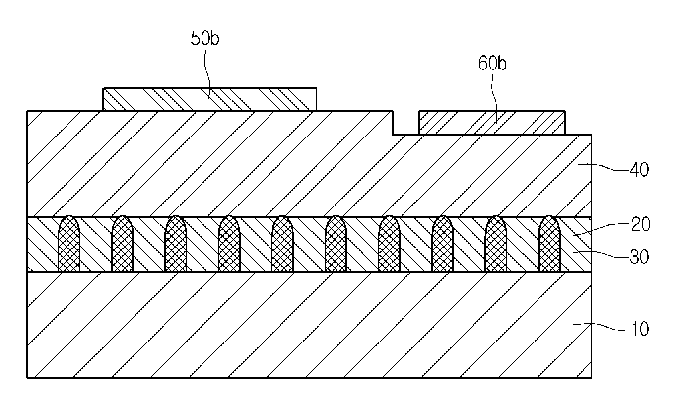
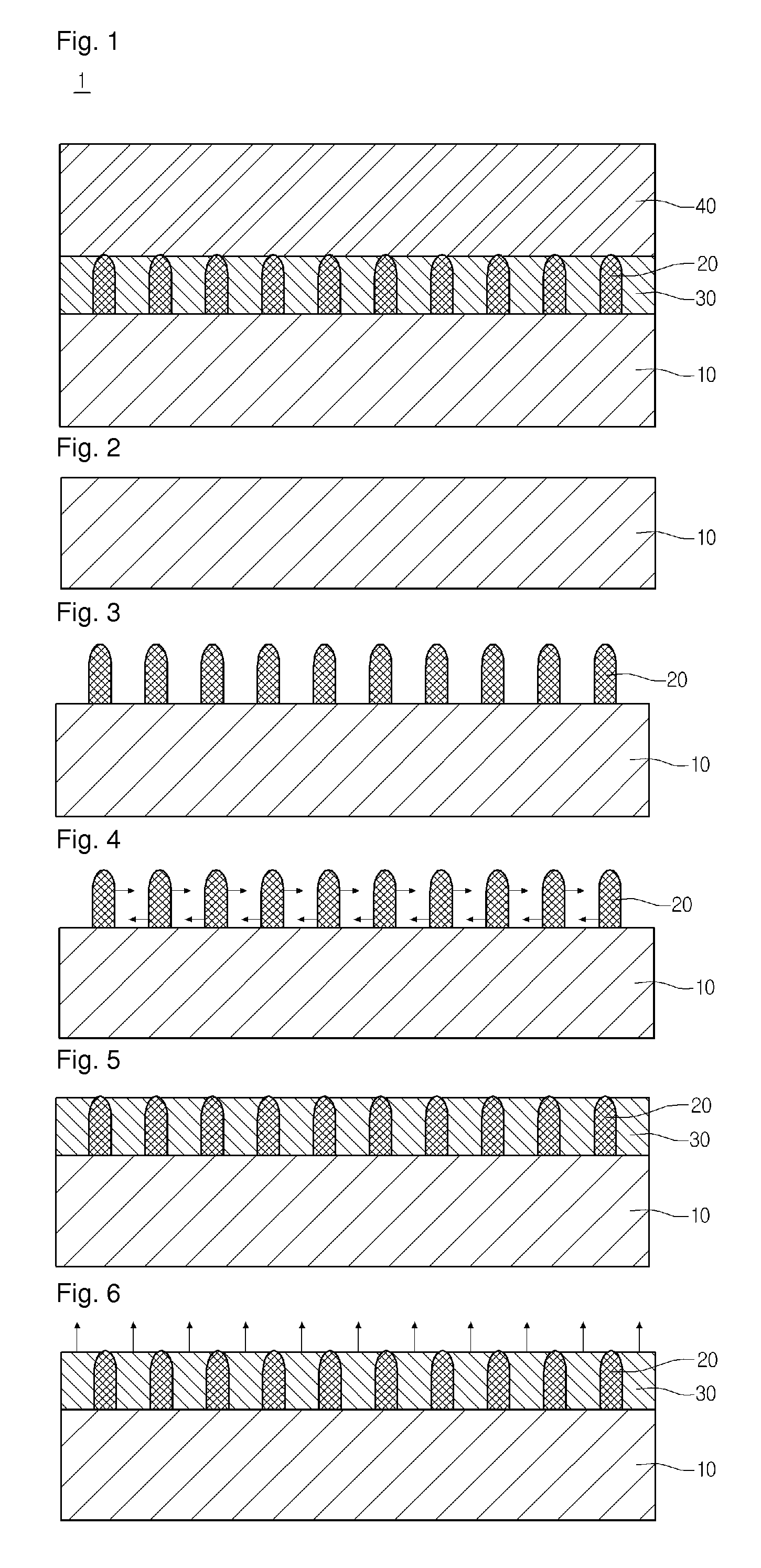
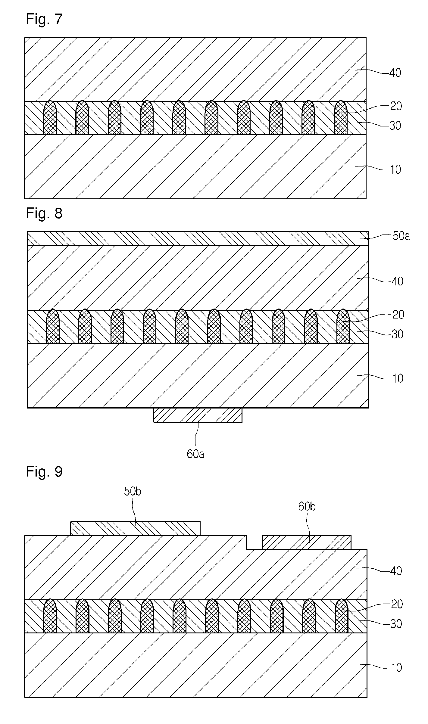
[0026]Referring to FIG. 1, a semiconductor device 1 may include a pattern 20, a buffer layer 30, and an epitaxial layer 40 on a base substrate 10.

[0027]The base substrate 10 may be formed of silicon carbide. The silicon carbide has a band gap and thermal conductivity greater than those of silicon. Also, the silicon carbide has carrier mobility similar to that of the silicon and a saturated electron drift velocity and pressure resistance greater than those of the silicon. Thus, the silicon carbide may be applied to a semiconductor device for which high efficiency, high pressure resistance, and high capacity are required.

[0028]The self-assembled pattern 20 is grown on the base substrate 10. The self-assembly represents a phenomenon in which components of molecules voluntarily form a well-ordered structure without artificially manipulating the respective molecules. When the base substrate 10 containing the silicon carbide is exposed to a carbon compound gas, the self-assembled pattern...

second embodiment

[0053]Referring to FIG. 10, in a semiconductor device 2 an epitaxial layer 130 may be disposed on a base substrate 110 including a pattern groove 120.

[0054]The base substrate 110 may be formed of silicon carbide. The silicon carbide has a band gap and thermal conductivity greater than those of silicon. Also, the silicon carbide has carrier mobility similar to that of the silicon and a saturated electron drift velocity and pressure resistance greater than those of the silicon. Thus, the silicon carbide may be applied to a semiconductor device for which high efficiency, high pressure resistance, and high capacity are required.

[0055]The pattern groove 120 is defined in the base substrate 110. A defect of the epitaxial layer 130 directly disposed on the base substrate 110 may be significantly reduced through the pattern groove 120.

[0056]Specifically, the base substrate 110 formed of the silicon carbide has a basal plane dislocation (BPD) 102. Since the BPD 102 greatly affects reliabili...


PUM

PropertyMeasurementUnit
heightaaaaaaaaaa
diameteraaaaaaaaaa
humidityaaaaaaaaaa

Abstract

A semiconductor device comprises a base substrate, a pattern on the base substrate, a buffer layer on the base substrate, and an epitaxial layer on the buffer. The pattern is a self-assembled pattern. A method for growing a semiconductor crystal comprises cleaning a silicon carbide substrate, forming a self-assembled pattern on the silicon carbide substrate, forming a buffer layer on the silicon carbide substrate, and forming an epitaxial layer on the buffer layer. A semiconductor device comprises a base substrate comprising a pattern groove and an epitaxial layer on the base substrate. A method for growing a semiconductor crystal comprises cleaning a silicon carbide substrate, forming a self-assembled projection on the silicon carbide substrate, forming a pattern groove in the silicon carbide, and forming an epitaxial layer on the silicon carbide.

Description

CROSS-REFERENCE TO RELATED APPLICATIONS[0001]This application is the U.S. national stage application of International Patent Application No. PCT / KR2012 / 000571, filed Jan. 20, 2012, which claims priority to Korean Application Nos. 10-2011-0007518, filed Jan. 25, 2011, and 10-2011-0010962, filed Feb. 8, 2011, the disclosures of each of which are incorporated herein by reference in their entirety.TECHNICAL FIELD[0002]The present disclosure relates to a semiconductor device and a method for growing a semiconductor crystal.BACKGROUND ART[0003]In a semiconductor substrate supporting a semiconductor device, the greatest research projects for improving efficiency and properties of the semiconductor device are to reduce crystal defects of a semiconductor layer grown on the substrate and improve crystalline of the semiconductor layer.[0004]A buffer layer may be formed to reduce dislocation defects in a crystal growth process. To form the buffer layer, a process of forming a pattern on a surfa...

Claims


Application Information

Patent Timeline
Patent Type & Authority Patents(United States)
IPC IPC(8): H01L29/16H01L21/02H01L31/0312
CPCH01L29/1608H01L21/0243H01L21/0262H01L21/02378H01L21/02447H01L21/02529H01L21/02617H01L21/02634H01L21/02639H01L21/02647H01L21/02658
Inventor KIM, MOO SEONGJO, YEONG DEUKSON, CHANG HYUNKIM, BUM SUP
Owner LX SEMICON CO LTD
Learn More