
Method for etching atomic layer of graphene

a graphene layer and graphene technology, applied in the field of atomic layer etching method of graphene, can solve the problems of inability to adjust and position the graphene layer, contact failure between the graphene of the channel portion and the metal of the source/drain electrode, and inability to commercialize for various purposes. , to achieve the effect of minimizing physical and electrical damage to the graphen

Active Publication Date: 2016-01-26
RES & BUSINESS FOUND SUNGKYUNKWAN UNIV
View PDF7 Cites 8 Cited by
  • Summary
  • Abstract
  • Description
  • Claims
  • Application Information

AI Technical Summary

Benefits of technology

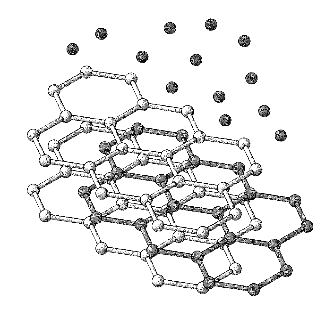
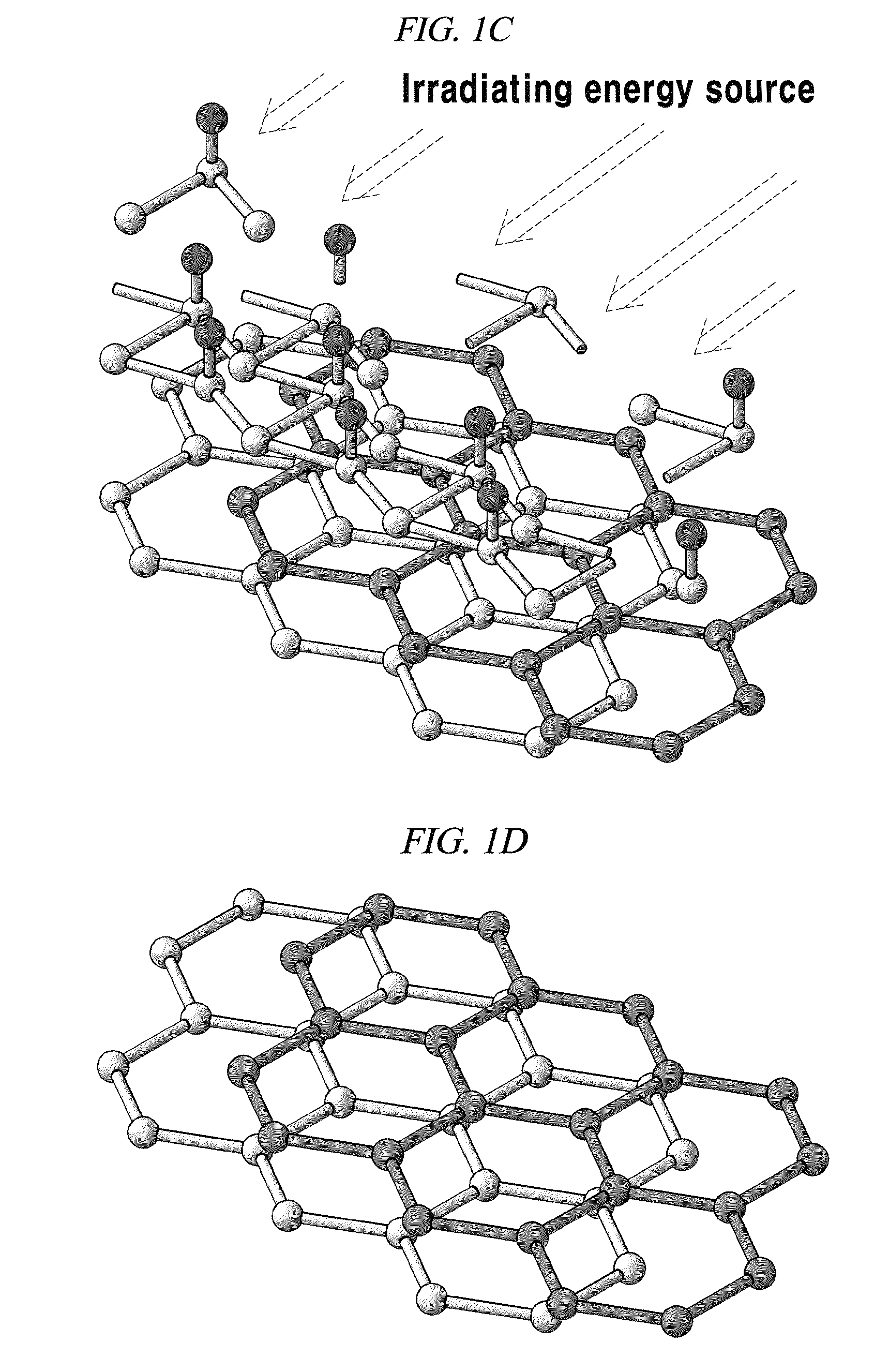
The patent text describes a method for etching graphene using atomic layer etching (ALE) which minimizes damage to the graphene. This method can be used in the production of devices made from graphene, such as transistors or sources / drain electrodes, which require a multiple number of stacked graphene layers. The ALE method is simple and cost-effective and avoids the risk of contamination during the etching process. The method involves adsorbing reactive radicals onto the surface of the graphene and irradiating it with an energy source to remove a small amount of material. This results in a cleaner reaction chamber and reduces the risk of contamination. The technical effects of this patent text include improved efficiency and accuracy in etching graphene with minimal damage using a simple and cost-effective method.

Problems solved by technology

In conventional methods of producing an exfoliated graphene, however, adjustment and positioning of graphene layers have been impossible.
Thus, the exfoliated graphene produced by conventional methods has a problem in that it is less suitable to be commercialized for various purposes.
However, in case of a device having only a channel portion of which is formed of graphene produced by the CVD method or the like, there may occur a contact failure between the graphene of the channel portion and a metal of source / drain electrodes.
Thus, degradation of a device characteristic may be caused.
According to these atomic layer etching methods for graphene, however, adjusting a graphene layer is not easy.
Particularly, the atomic layer etching method for graphene using O2 plasma has a drawback in that oxygen may remain at the edge of the graphene after the graphene is etched, thus affecting characteristics of the graphene.
For example, when adsorbing the reactive radicals onto the surface of the graphene by using a neutral beam including reactive radicals, it may be difficult to avoid contamination by carbon and metal due to the presence of a reflecting plate within an etching chamber.

Method used


Image

  • Method for etching atomic layer of graphene
  • Method for etching atomic layer of graphene
  • Method for etching atomic layer of graphene

Examples


examples

[0078]1. Method for Performing Atomic Layer Etching of Graphene and Analysis Thereof

[0079]In this example, in order to generate O2 radicals as reactive radicals to be adsorbed onto a surface of graphene, a RF power (13.56 MHz) of about 300 W was applied to an ICP plasma source. Further, the O2 radicals were designed to reach the surface of the sample by pumping flow.

[0080]Meanwhile, in order to produce an Ar neutral beam as an energy source to be irradiated to the graphene on which the reactive radicals were adsorbed, a RF power (13.56 MHz) of about 300 W was applied to the ICP plasma source. Here, the Ar neutral beam was produced by using a low angle forward reflected neutral (LAFRN) beam technique. The LAFRN beam technique is a method for extracting an Ar neutral beam by using a three grid system and a reflector after producing ICP-type plasma.

[0081]To adjust energy of the Ar neutral beam, the three grid system including a first to a third grid was utilized. Here, the first grid w...


PUM

PropertyMeasurementUnit
contact resistanceaaaaaaaaaa
frequencyaaaaaaaaaa
frequencyaaaaaaaaaa

Abstract

This present disclosure relates to an atomic layer etching method for graphene, including adsorbing reactive radicals onto a surface of the graphene and irradiating an energy source to the graphene on which the reactive radicals are adsorbed.

Description

CROSS-REFERENCE TO RELATED APPLICATIONS[0001]This application is a continuation of International Application No. PCT / KR2012 / 005747 filed on Jul. 19, 2012, claiming the priority based on Korean Patent Application No. 10-2011-0072843 filed on Jul. 22, 2011 and Korean Patent Application No. 10-2012-0074309 filed on Jul. 9, 2012, the contents of all of which are incorporated herein by reference in their entirety for all purposes.BACKGROUND[0002]1. Field[0003]The various embodiments described herein pertain generally to an atomic layer etching method for graphene, including adsorbing reactive radicals onto a surface of the graphene and irradiating an energy source to the graphene on which the reactive radicals are adsorbed.[0004]2. Description of Related Art[0005]Exfoliated graphene has excellent physical and electrical characteristics. Due to these advantages, research on graphene has been actively conducted. In conventional methods of producing an exfoliated graphene, however, adjustme...

Claims


Application Information

Patent Timeline
Patent Type & Authority Patents(United States)
IPC IPC(8): H01L21/302H01L29/66H01L21/04H01L29/16
CPCH01L21/042H01L21/0405H01L29/1606H01L29/66037H01L21/3065C01B32/05B01J19/084B01J19/12C01B32/19C01B32/194C01B2204/04
Inventor YEOM, GEUN YOUNGLIM, WOONG SUNMIN, KYUNG SEOKKIM, YI YEONOH, JONG SIK
Owner RES & BUSINESS FOUND SUNGKYUNKWAN UNIV
Learn More