Semiconductor device comprising a main region, a current sense region, and a well region
a technology of a main region and a well region, which is applied in the direction of the device, the electrical apparatus, the basic electric element, etc., can solve the problems of low breakdown resistance and achieve the effect of enhancing breakdown resistan
- Summary
- Abstract
- Description
- Claims
- Application Information
AI Technical Summary
Benefits of technology
Problems solved by technology
Method used
Image
Examples
embodiment 1
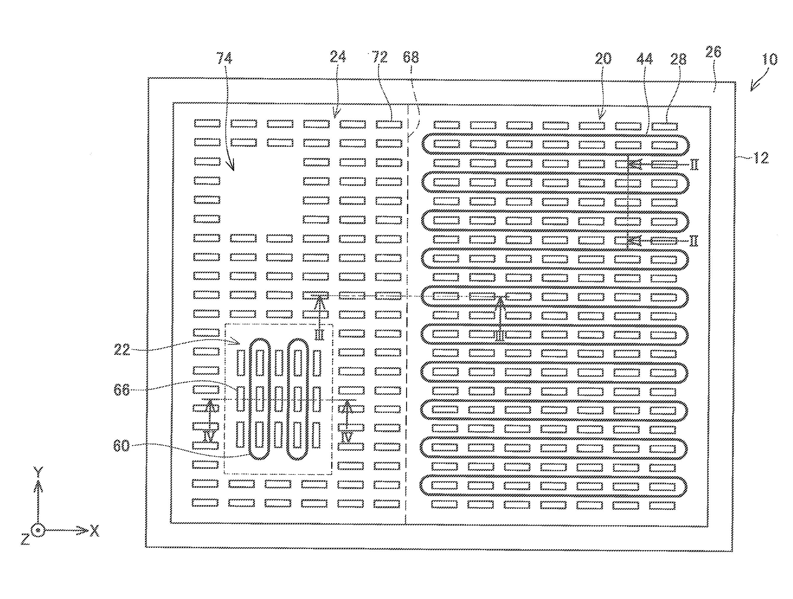
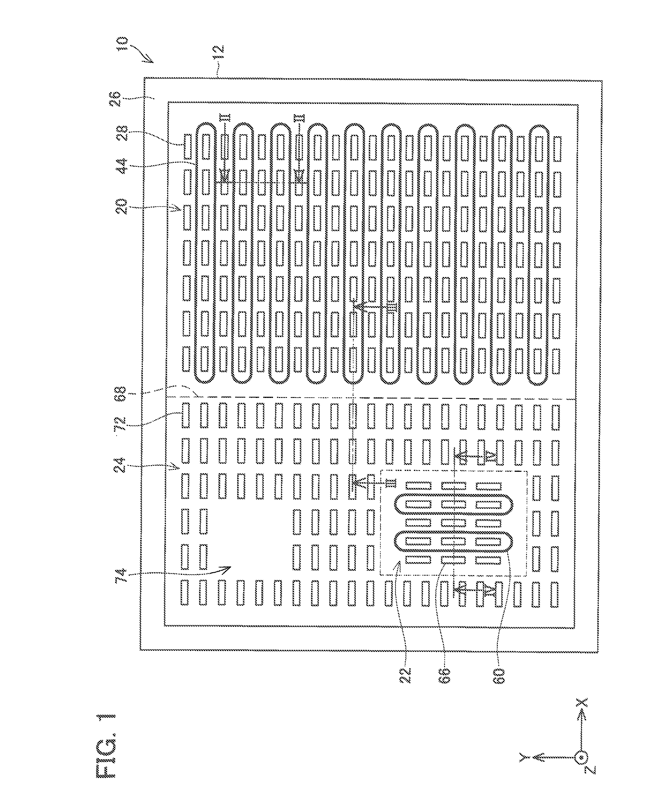
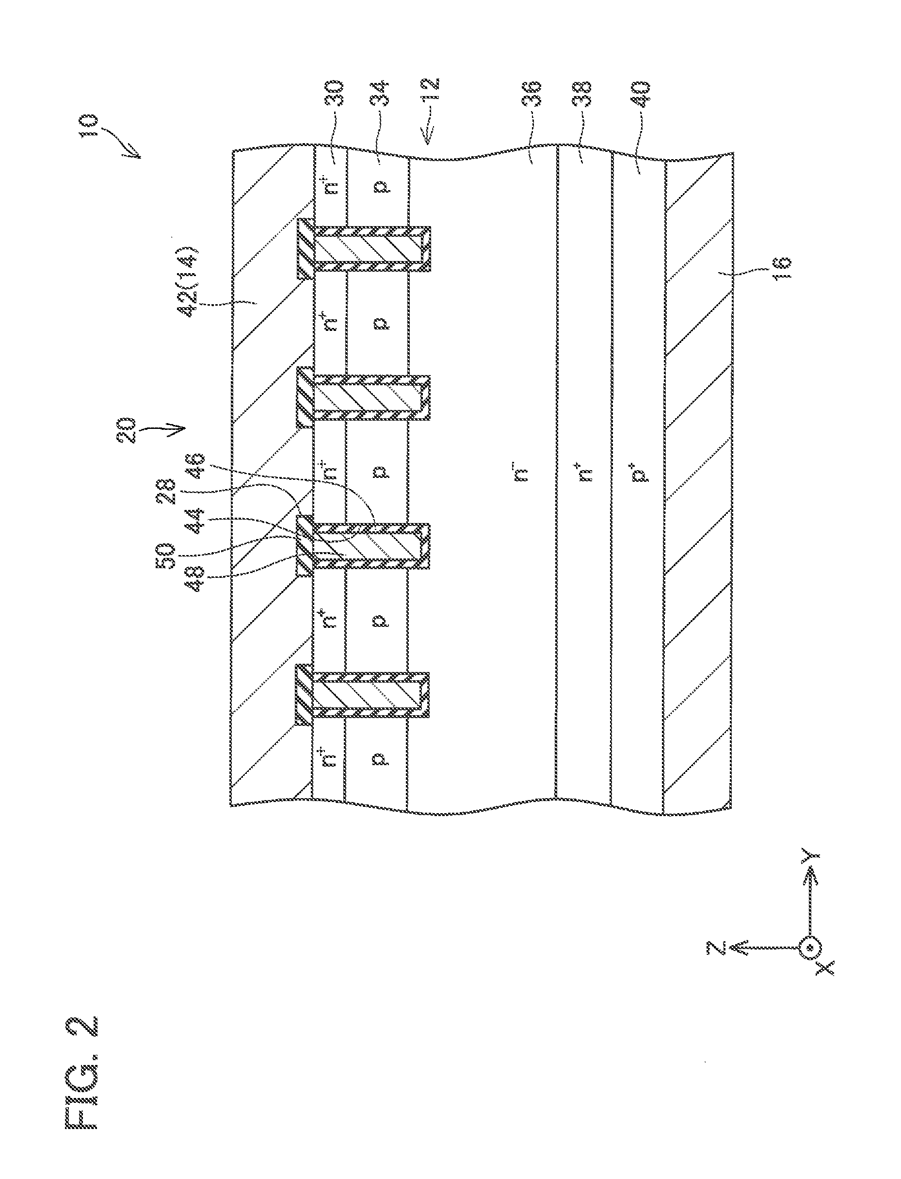
[0026]A semiconductor device 10 of the present embodiment is described below with reference to FIGS. 1 to 4. As shown in FIGS. 2 to 4, the semiconductor device 10 includes a semiconductor substrate 12, an upper electrode 14, and a lower electrode 16. The semiconductor substrate 12 is a substrate made of silicon or made of silicon carbide. The upper electrode 14 is formed on an upper surface of the semiconductor substrate 12. The lower electrode 16 is formed on a lower surface of the semiconductor substrate 12. It should be noted that for a clearer illustration, FIG. 1 omits to show the upper electrode 14.
[0027]As shown in FIG. 1, the semiconductor substrate 12 includes a main region 20, a current sense region 22, a well region 24, and a peripheral region 26. The main region 20 and the current sense region 22 both function as IGBTs. The main region 20 and the well region 24 are disposed adjacent to each other in an X direction (i.e. a left-to-right direction of FIG. 1). Further, the ...
embodiment 2
[0053]A semiconductor device 100 of the present embodiment is described below with reference to FIGS. 5 to 9. It should be noted that those components of the semiconductor device 100 of the present embodiment which are the same as those of the semiconductor device 10 of Embodiment 1 are given the same reference signs, and as such, are not described below in detail. As shown in FIGS. 6 to 9, the semiconductor device 100 includes a semiconductor substrate 102, an upper electrode 104, and a lower electrode 16. It should be noted that for a clearer illustration, FIG. 5 omits to show the upper electrode 104.
[0054]As shown in FIG. 5, the semiconductor substrate 102 includes a main region 106, a current sense region 108, a well region 110, and a peripheral region 26. The main region 106 and the current sense region 108 both function as IGBTs. The main region 106 and the well region 110 are disposed adjacent to each other in an X direction (i.e. a left-to-right direction of FIG. 5). Further...
embodiment 3
[0074]A semiconductor device 200 of the present embodiment is described below with reference to FIGS. 10 to 12. It should be noted that those components of the semiconductor device 200 of the present embodiment which are the same as those of the semiconductor device 10 of Embodiment 1 or those of the semiconductor device 100 of Embodiment 2 are given the same reference signs, and as such, are not described below in detail. As shown in FIGS. 11 and 12, the semiconductor device 200 includes a semiconductor substrate 202, an upper electrode 104, and a lower electrode 16.
[0075]As shown in FIG. 10, the semiconductor substrate 202 includes a main region 204, a current sense region 206, a well region 208, and a peripheral region 26. The main region 204 and the current sense region 206 both function as IGBTs. The main region 204 and the well region 208 are disposed adjacent to each other in an X direction (i.e. a left-to-right direction of FIG. 10). Further, the well region 208 is disposed ...
PUM
 Abstract
Description
Claims
Application Information
 - R&D
- Intellectual Property
- Life Sciences
- Materials
- Tech Scout
- Unparalleled Data Quality
- Higher Quality Content
- 60% Fewer Hallucinations
Browse by: Latest US Patents, China's latest patents, Technical Efficacy Thesaurus, Application Domain, Technology Topic, Popular Technical Reports.
© 2025 PatSnap. All rights reserved.Legal|Privacy policy|Modern Slavery Act Transparency Statement|Sitemap|About US| Contact US: help@patsnap.com


