Three dimensional stacked semiconductor structure and method for manufacturing the same

a three-dimensional stacked, semiconductor technology, applied in semiconductor devices, semiconductor/solid-state device details, electrical devices, etc., can solve the problems of time-consuming, expansive, and inability to respond to the 3d stacked semiconductor structure effectively, and achieve the effect of simple manufacturing procedures, increased structure operation speed, and reduced resistan

Active Publication Date: 2015-09-15
MACRONIX INT CO LTD
View PDF25 Cites 2 Cited by
  • Summary
  • Abstract
  • Description
  • Claims
  • Application Information

AI Technical Summary

Benefits of technology

[0006]The disclosure relates to a three-dimensional (3D) stacked semiconductor structure and method of manufacturing the same. The resistance of the 3D stacked semiconductor structure could be effectively reduced by simple manufacturing procedures provided in the embodiments, and the operation speed of the structure is consequently increased. Accordingly, the 3D stacked semiconductor structure provided in the embodiments have low production cost due to simple and quick manufacturing steps, and the applied memory possesses improved speed, and high and stable performance.

Problems solved by technology

High resistances of the polysilicon layers 133 would have considerable effect on the programming speed (e.g. read latency) of the 3D stacked flash memory, such as causing response delay or even out of operation.
Currently, the polysilicon layers 133 in the fan-out region 13 are ion implanted layer by layer, which is time-consuming and expansive.

Method used


Image

  • Three dimensional stacked semiconductor structure and method for manufacturing the same
  • Three dimensional stacked semiconductor structure and method for manufacturing the same
  • Three dimensional stacked semiconductor structure and method for manufacturing the same

Examples


Embodiment Construction

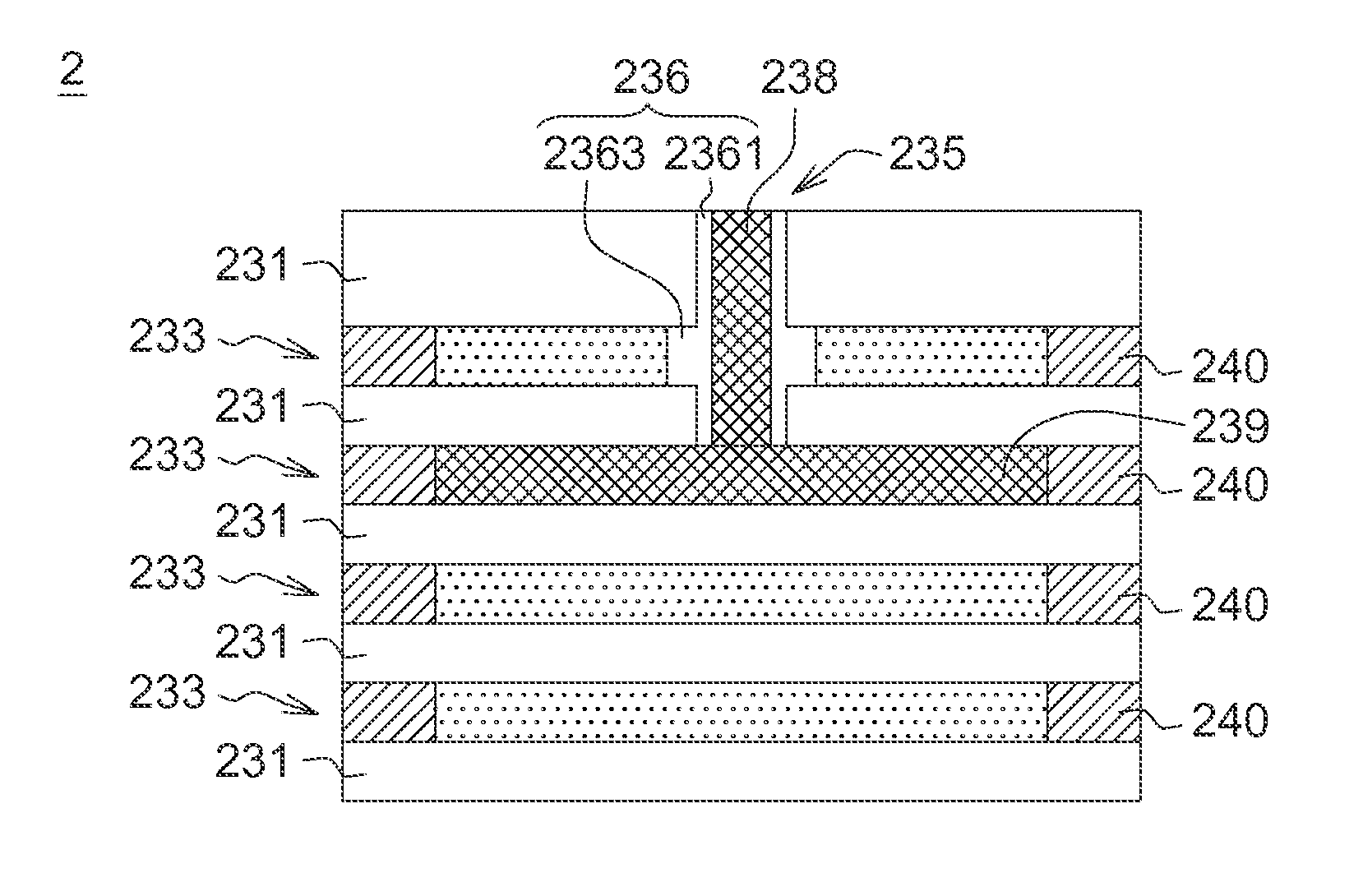
[0016]In the embodiments of the present disclosure, a three-dimensional (3D) stacked semiconductor structure and method of manufacturing the same are provided. The 3D stacked semiconductor structure of the embodiments possess the reduced resistance, particularly the resistance of bit lines which the operation current passes through, thereby effectively increasing the speed of the 3D flash memory of application. Also, the 3D stacked semiconductor structure of the embodiments are manufactured by simple process, and adopting no time-consuming and expensive procedures such as several ion-implant procedures. Accordingly, the 3D stacked semiconductor structure provided in the embodiments have low production cost due to simple and quick manufacturing steps, and the applied memory possesses improved speed, and high and stable performance.

[0017]The embodiments below are disclosed for elaborating the 3D stacked semiconductor structures of the disclosure and method of manufacturing the same. H...


PUM


Abstract

A three dimensional stacked semiconductor structure comprises a stack including plural oxide layers and conductive layers arranged alternately, at least a contact hole formed vertically to the oxide layers and the conductive layers, and extending to one of the conductive layers, an insulator formed at the sidewall of the contact hole, a conductor formed in the contact hole and connecting the corresponding conductive layer, and the corresponding conductive layer comprises a silicide. The silicide could be formed at edges or an entire body of the corresponding conductive layer. Besides the silicide, the corresponding conductive layer could, partially or completely, further comprise a conductive material connected to the conductor. The corresponding conductive layer which the contact hole extends to has higher conductivity than other conductive layers. Also, the 3D stacked semiconductor structure could be applied to a fan-out region of a 3D flash memory.

Description

BACKGROUND[0001]1. Field of the Invention[0002]The disclosure relates in general to a three-dimensional (3D) stacked semiconductor structure and method of manufacturing the same, and more particularly to the 3D stacked semiconductor structure in a fan-out region of a 3D flash memory and method of manufacturing the same.[0003]2. Description of the Related Art[0004]A nonvolatile semiconductor memory device is typically designed to securely hold data even when power is lost or removed from the memory device. Various types of nonvolatile memory devices have been proposed in the related art. Also, manufactures have been looking for new developments or techniques combination for stacking multiple planes of memory cells, so as to achieve greater storage capacity. For example, several types of multi-layer stackable thin-film transistor (TFT) NAND-type flash memory structures have been proposed.[0005]With the development of size reduction of device, the distance between gates in the array re...

Claims


Application Information

Patent Timeline
Patent Type & Authority Patents(United States)
IPC IPC(8): H01L27/115H01L21/768H01L23/522
CPCH01L27/11575H01L21/76805H01L21/76831H01L21/76877H01L21/76889H01L27/11548H01L23/5226H01L27/11556H01L27/11582H01L2924/0002H10B41/50H10B41/27H10B43/50H10B43/27H01L2924/00
Inventor LAI, ERH-KUNSHIH, YEN-HAO
Owner MACRONIX INT CO LTD
Why Eureka
Try Eureka