Gate driving waveform control
a technology of driving waveform and gate, applied in the field of liquid crystal display, can solve the problems of large circuit area, high cost, disadvantageous association of high frequency with complex circuitry, etc., and achieve the effect of increasing complexity, area and cost in circuitry
- Summary
- Abstract
- Description
- Claims
- Application Information
AI Technical Summary
Benefits of technology
Problems solved by technology
Method used
Image


Examples
first embodiment
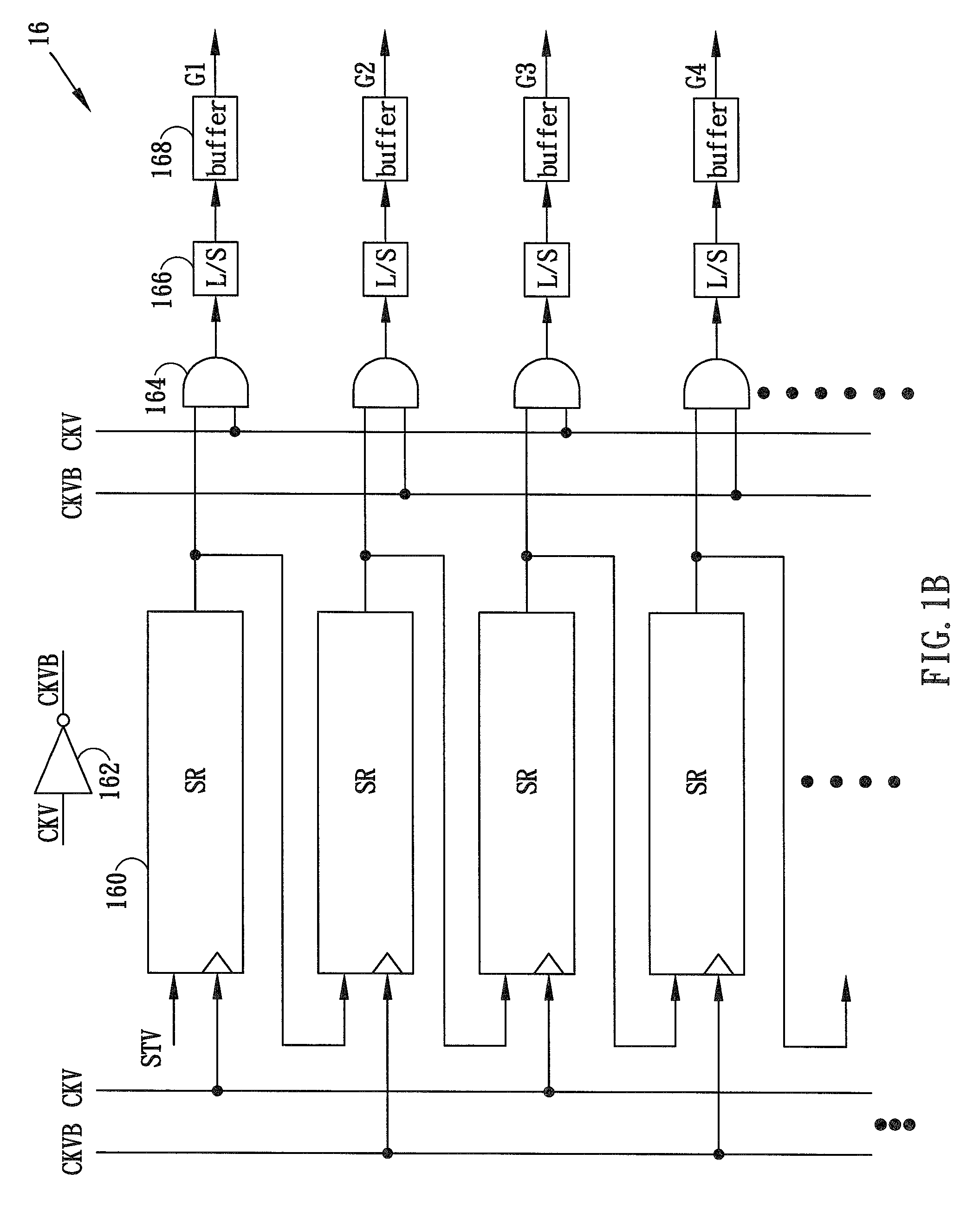
[0020]FIG. 1B illustrates a detailed circuit of the gate driver 16 in FIG. 1A according to the present invention, and FIG. 1C shows a timing diagram illustrating the resultant gate driving waveforms associated with the gate driver 16 of FIG. 1B.
[0021]In the embodiment, the gate driver 16 primarily includes a number of shift registers (SR) 160. Each shift register 160 has an input terminal for receiving an input signal, a clock terminal for receiving a clock signal, and an output terminal for producing an output signal. The shift register 160 is utilized to transfer or shift the input signal to the output terminal in response to each clock signal. The shift register 160 may be implemented, for example, by a D-type flip-flop. According to the embodiment, the first (topmost) shift register 160 receives the vertical synchronization signal STV, while the second (and following) shift register 160 is coupled to receive the output signal of a previous shift register 160. The odd-number shif...
second embodiment
[0023]FIG. 1D illustrates a detailed circuit of the gate driver 16 in FIG. 1A according to the present invention, and FIG. 1E shows a timing diagram illustrating the resultant gate driving waveforms associated with the gate driver 16 of FIG. 1D.
[0024]In the embodiment, the gate driver 16 has a structure similar to that in FIG. 1B, except that no logic circuits (for example, the AND gates 164 in FIG. 1B) are used. The comprising elements, such as the shift registers 160, the level shifters 166 and the output buffers 168 are coupled and operated in the same manner as those in FIG. 1B, except that the outputs of the shift registers 160 are directly coupled to the level shifters 166. Therefore, corresponding discussion is omitted here for brevity. As the logic circuits 164 (FIG. 1B) are not used in this embodiment to control the phase relationship between the resultant gate driving waveform G1-G4 and the horizontal synchronization signal CKV, the resultant gate driving signals G1-G2m ac...
third embodiment
[0026]FIG. 2B illustrates detailed circuits of the gate driver A 16 and the gate driver B 18 in FIG. 2A according to the present invention, and FIG. 2C shows a timing diagram illustrating the resultant gate driving waveforms associated with the gate drivers 16 / 18 of FIG. 2B.
[0027]In the embodiment, the gate driver A 16 has a structure similar to that in FIG. 1B, except that all shift registers 160 operate under the direct control of the horizontal synchronization signal CKV, and all the logic circuits (such as logic AND gates) 164 receive the horizontal synchronization signal CKV. Accordingly, the gate driver A 16 generates odd-number gate driving signals G1, G3 etc. which have the same waveforms as those in FIG. 1C, and are reproduced in FIG. 2C. With respect to the other gate driver B 18, it has a structure similar to the gate driver A 16 (FIG. 2B), except that all shift registers 160 operate under the direct control of the inverted horizontal synchronization signal CKVB, and all ...
PUM
 Abstract
Description
Claims
Application Information
 - R&D
- Intellectual Property
- Life Sciences
- Materials
- Tech Scout
- Unparalleled Data Quality
- Higher Quality Content
- 60% Fewer Hallucinations
Browse by: Latest US Patents, China's latest patents, Technical Efficacy Thesaurus, Application Domain, Technology Topic, Popular Technical Reports.
© 2025 PatSnap. All rights reserved.Legal|Privacy policy|Modern Slavery Act Transparency Statement|Sitemap|About US| Contact US: help@patsnap.com