Electro-optic device and electronic apparatus

a technology of optical devices and electronic devices, applied in non-linear optics, instruments, optics, etc., can solve the problems of limit of thinning the film thickness using a polishing process, etc., and achieve the effect of reducing the number of scratches

Active Publication Date: 2015-09-01
SEIKO EPSON CORP
View PDF13 Cites 0 Cited by
  • Summary
  • Abstract
  • Description
  • Claims
  • Application Information

AI Technical Summary

Benefits of technology

The patent describes a method for manufacturing an electro-optic device with improved display quality. The method includes steps to form a concave portion on the surface of the pixel electrode, cover the concave portion with a second insulating film, and planarize the second insulating film to reduce the size of the cavity formed in the second insulating film. The second insulating film is made thin by reducing the position of the apex of the cavity, which helps to reduce deterioration in the display signal and provide a high quality display. Additionally, the method includes steps to reduce minute scratches on the polished surface of the second insulating film, making it a further planar surface.

Problems solved by technology

In the liquid crystal device which is disclosed in JP-A-2011-164249, it is necessary to make a film thickness of the insulating film which is arranged between the pixel electrode and the alignment film small after polishing since an effective voltage which is applied to a liquid crystal between the pixel electrode and the common electrode is decreased, however, there has been a limit to thinning the film thickness using a polishing process.
Specifically, when the insulating film becomes excessively thin using the polishing process, the cavity is exposed, and alignment of the liquid crystal is disturbed in a region in which the cavity is exposed, therefore there has been a limit of thinning the film thickness using the polishing process.

Method used


Image

  • Electro-optic device and electronic apparatus
  • Electro-optic device and electronic apparatus
  • Electro-optic device and electronic apparatus

Examples


embodiment

Schematic Description of Electro-Optic Device

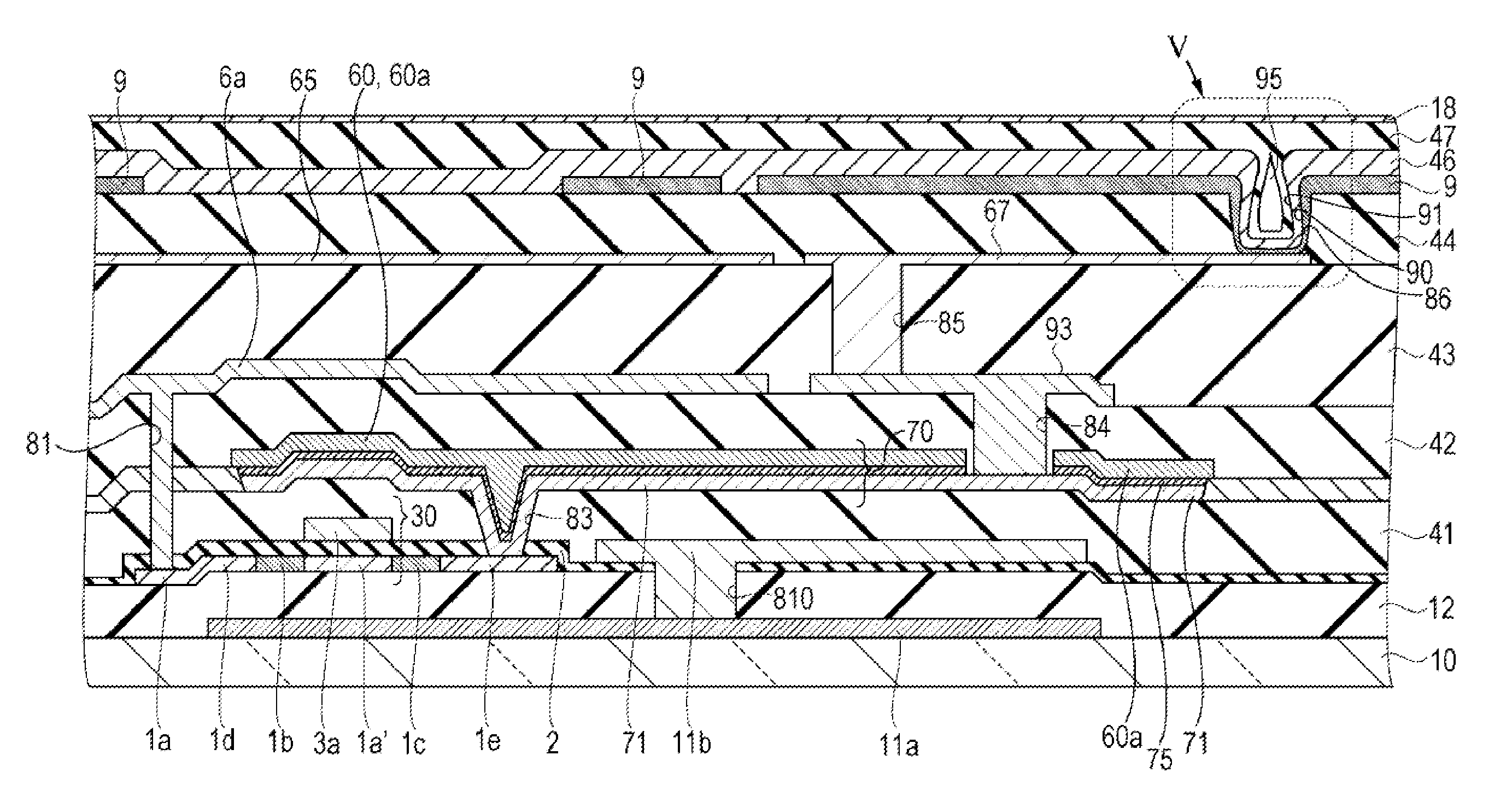
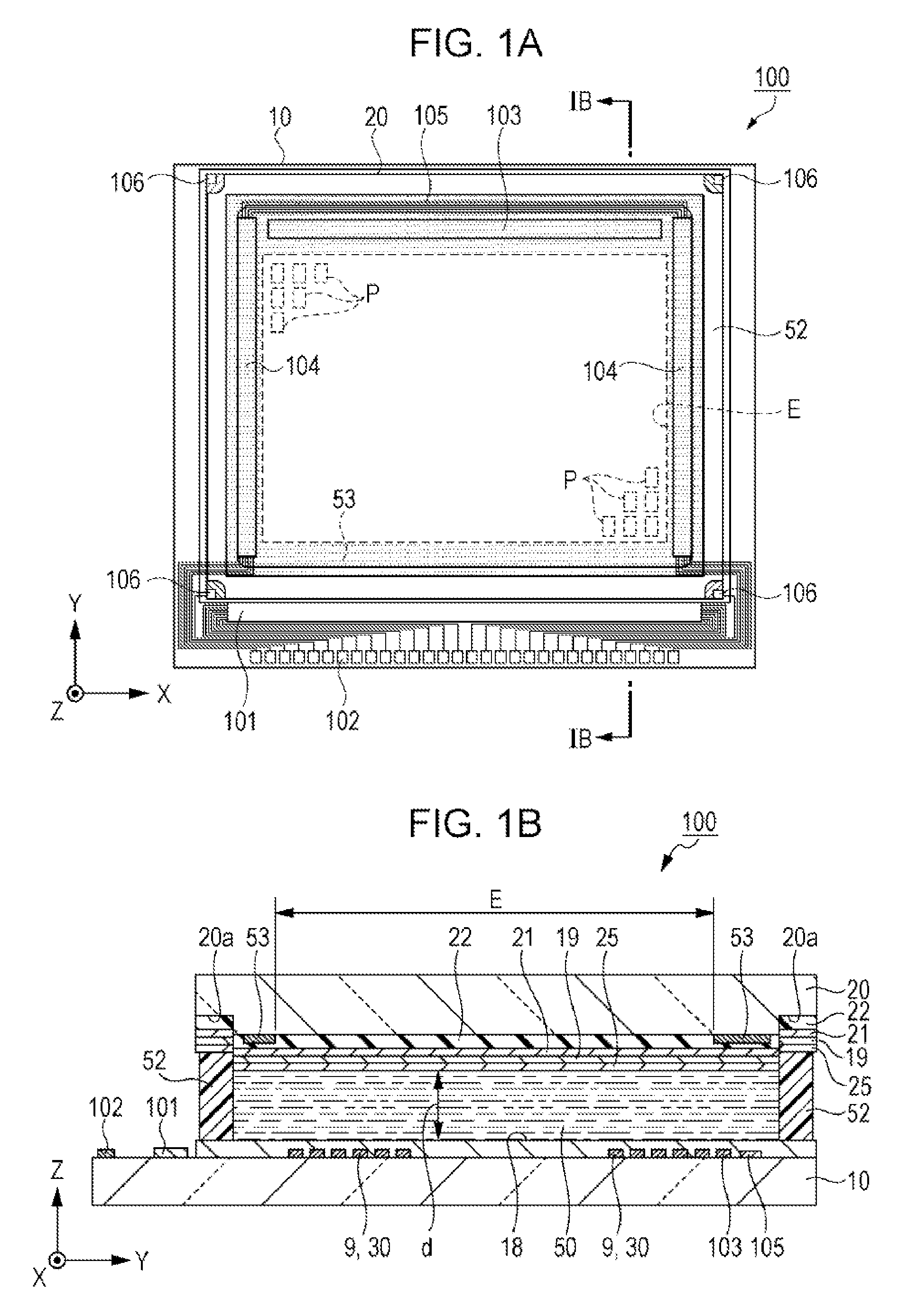
[0031]A liquid crystal device 100 as an example of an electro-optic device according to the embodiment is a reflection type liquid crystal device which includes a thin film transistor (hereinafter, referred to as TFT) 30 as an example of a pixel switching element. The liquid crystal device 100 can be preferably used, for example, as a reflection type optical modulation device of a liquid crystal projector which will be described later.

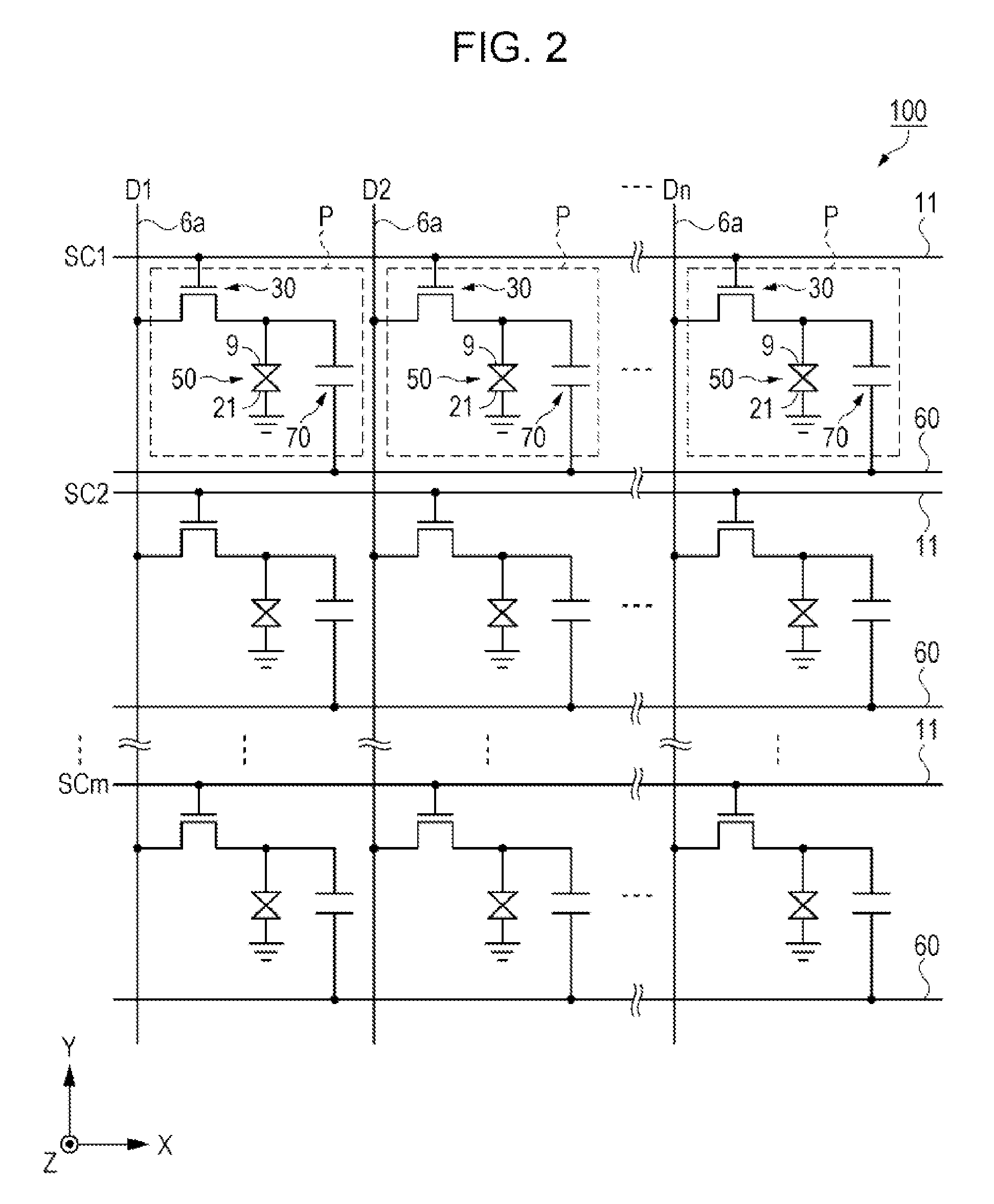
[0032]First, the entire configuration of the liquid crystal device 100 according to the embodiment will be described with reference to FIGS. 1A, 1B, and 2.

[0033]FIG. 1A is a schematic plan view which illustrates a configuration of the liquid crystal device, FIG. 1B is a schematic cross-sectional view of the liquid crystal device which is cut along IB-IB in FIG. 1A, and FIG. 2 is an equivalent circuit diagram which illustrates an electrical configuration of the liquid crystal device.

[0034]As illustrated in FI...

modification example 1

[0140]The embodiment of the invention is not limited to a reflection type liquid crystal device. For example, the embodiment can be applied to a transmission type liquid crystal device. In addition, the dielectric layer 46 may have a configuration in which transmissivity of the transmission type liquid crystal device is increased.

[0141]The dielectric layer 46 according to the embodiment of the invention is not essential, and a configuration may be adopted in which the dielectric layer 46 according to the embodiment is omitted and the contact hole 86 is covered with the pixel electrode 9. That is, it may be a configuration in which the dielectric layer 46 according to the embodiment is omitted and the side wall of the contact hole 86 is covered with the pixel electrode 9 which becomes thick toward the surface of the interlayer insulating film 44 (apex of contact hole 86) from the base of the contact hole 86.

[0142]In addition, the embodiment is not only applied to the liquid crystal d...


PUM


Abstract

Disclosed an electro-optic device which includes a reflective pixel electrode which is formed on a base of a contact hole in an approximately rectangular shape or an approximately oval shape, and a side wall thereof, and a second insulating film which covers the reflective pixel electrode, and has a cavity in the contact hole, in which the film thickness of the reflective pixel electrode becomes large toward the upper part from the base of the contact hole.

Description

BACKGROUND[0001]1. Technical Field[0002]The present invention relates to an electro-optic device, a method of manufacturing the electro-optic device, and an electronic apparatus on which the electro-optic device is mounted.[0003]2. Related Art[0004]A liquid crystal device as an example of an electro-optic device has a structure in which liquid crystal is interposed between a pair of substrates and in which one substrate between the pair of substrates is an element substrate including a Thin Film Transistor (hereinafter, briefly referred to as TFT) or a pixel electrode and the other substrate is a counter substrate which includes a common electrode with translucency.[0005]For example, a TFT, an interlayer insulating film, an electrode pixel, an insulating film, and an alignment film are laminated in this order on an element substrate of a liquid crystal device which is disclosed in JP-A-2011-164249. The TFT and the pixel electrode are connected through a contact hole which is formed ...

Claims


Application Information

Patent Timeline
IPC IPC(8): G02F1/136G02F1/1362G02F1/1335G02F1/1333
CPCG02F1/136227G02F1/133553G02F1/133345
Inventor IZAWA, SHOTARO
Owner SEIKO EPSON CORP
Why Eureka
Try Eureka