Method for producing group III nitride semiconductor light-emitting device
a technology of nitride and semiconductor light-emitting devices, which is applied in the manufacture of semiconductor/solid-state devices, semiconductor devices, electrical devices, etc., can solve the problems of poor adhesion of ag reflective films to the siosub>2 /sub>insulating films, and achieve the effect of preventing thermal migration, suppressing the reduction of reflective films, and preventing thermal migration
- Summary
- Abstract
- Description
- Claims
- Application Information
AI Technical Summary
Benefits of technology
Problems solved by technology
Method used
Image
Examples
embodiment 1
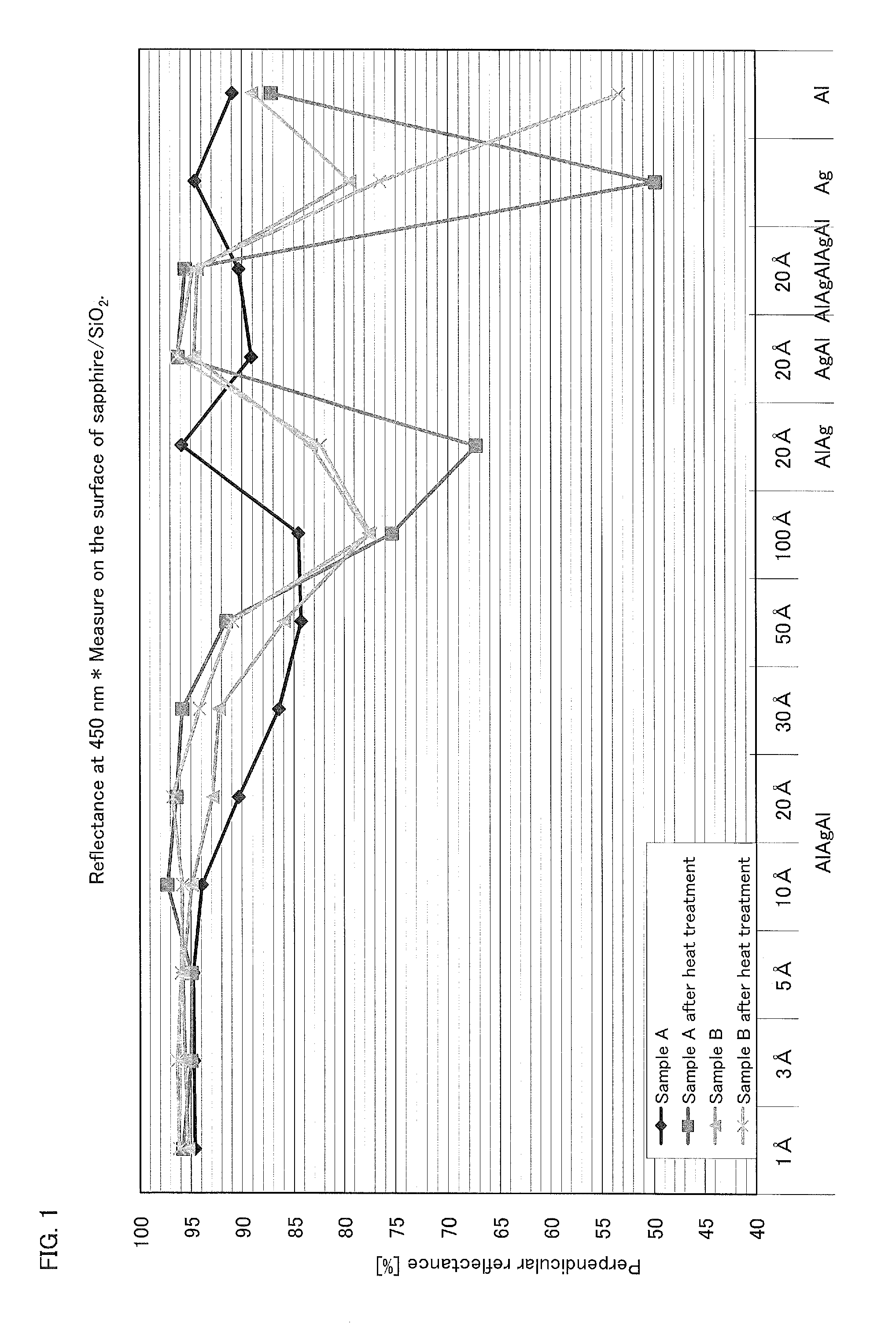
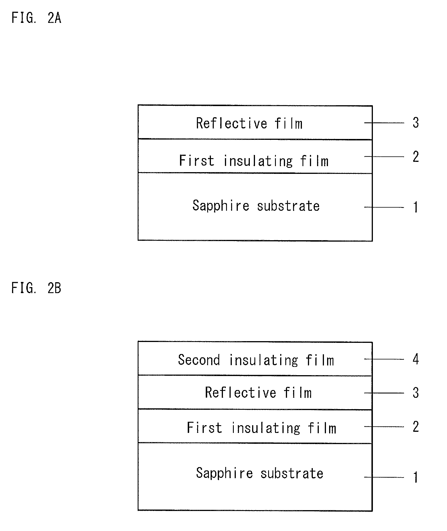
[0055]First, a first insulating film 2 (first insulator) formed of SiO2 having a thickness of 3000 Å was formed on a sapphire substrate 1, and a reflective film 3 of various materials was formed through deposition on the first insulating film 2, thereby producing sample A (refer to FIG. 2A). Thereafter, the reflectance was measured by letting a light perpendicularly incident to a surface of the reflective film in both cases where the heat treatment was performed or not. Similarly as above, a first insulating film 2, and a reflective film 3 were sequentially formed on a sapphire substrate 1, and further a second insulating film 4 of SiO2 (second insulator) having a thickness of 3000 Å was formed by CVD on the reflective film 3, thereby producing sample B (refer to FIG. 2B). Thereafter, the reflectance was measured in the same manner in both cases where the heat treatment was performed or not. Six types of materials were used as reflective films: Al / Ag / Al (means that an Al film, an Ag...
embodiment 2
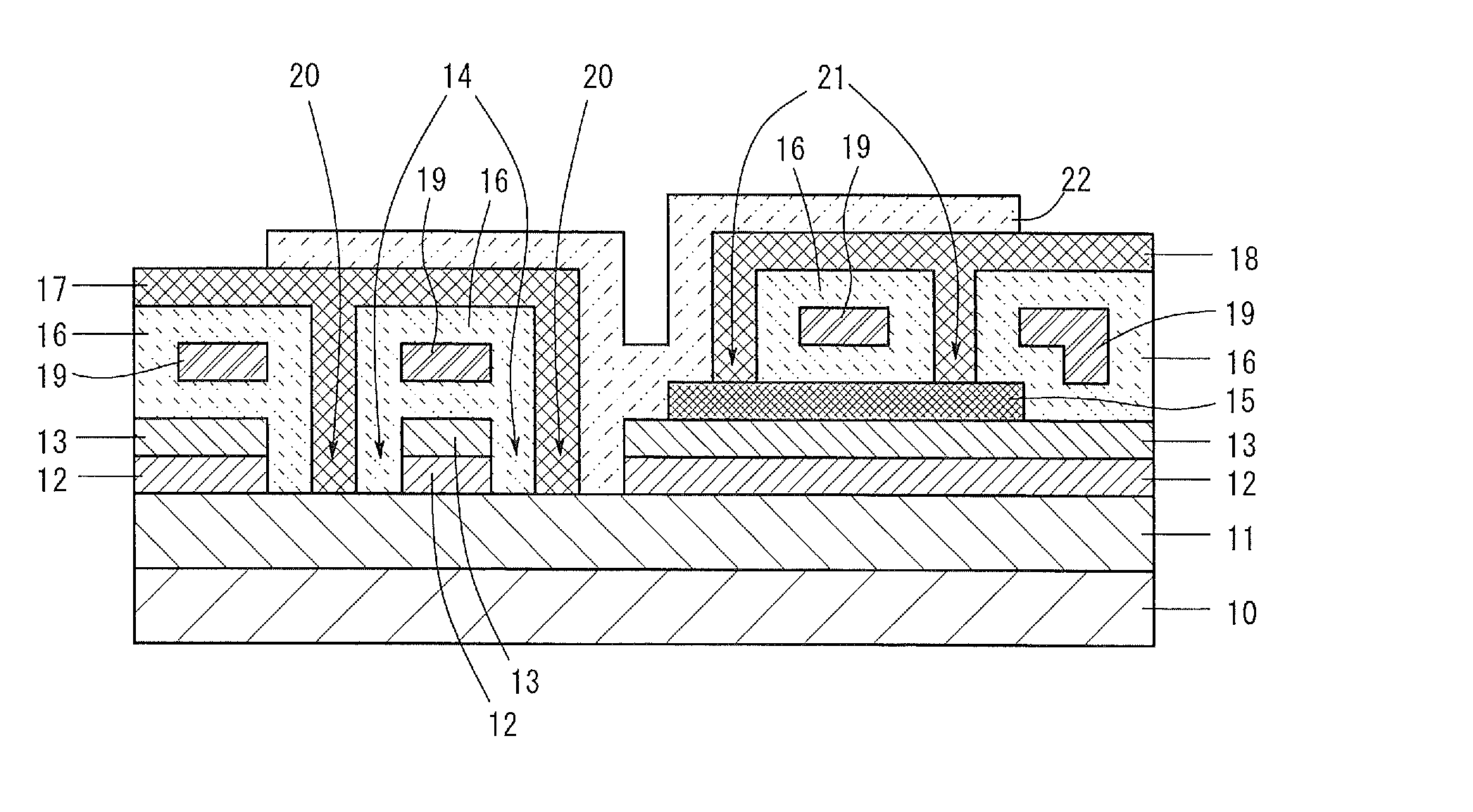
[0063]FIG. 4 is a plan view of the Group III nitride semiconductor light-emitting device according to Embodiment 2. FIG. 5 is an A-A cross-sectional view of the plan view shown in FIG. 4.
[0064]As shown in FIG. 4, the Group III nitride semiconductor light-emitting device according to Embodiment 2 comprises a sapphire substrate 10, and an n-GaN layer 11, a light-emitting layer 12, and a p-GaN layer 13 formed in this order on the sapphire substrate 10. At the center of the surface of the p-GaN layer 13, a plurality of holes 14 having a depth extending from the surface of the p-GaN layer 13 to the n-GaN layer 11 are formed in a linear pattern. An ITO electrode 15 is formed on almost the entire surface other than the region provided with the holes 14 of the surface of the p-GaN layer 13. Moreover, an insulating film 16 formed of SiO2 is provided so as to continuously cover the surface of the ITO electrode 15, the bottom and side surfaces of the holes 14, and the surfaces of the p-GaN lay...
embodiment 3
[0077]FIG. 7 shows a cross-sectional view of the structure of the Group III nitride semiconductor light-emitting device according to Embodiment 3. The Group III nitride semiconductor light-emitting device according to Embodiment 3 comprises a reflective film 119, an insulating film 120 of SiC2, and a solder layer 121 sequentially formed on the bottom surface of the sapphire substrate 10 (the side opposite to the surface having the n-GaN layer 11) of the Group III nitride semiconductor light-emitting device according to Embodiment 2. The reflective film 119 has the same structure of the reflective film 19 and comprises Al / Ag / Al. The respective Al has a thickness of 1 Å to 30 Å, and Ag has a thickness of 500 Å to 5000 Å. The solder layer 121 is formed of Au or AuSn.
[0078]The Group III nitride semiconductor light-emitting device according to Embodiment 3 is a face-up type device where light is extracted from the n-electrode 17 and the p-electrode 18 as in the Group III nitride semicond...
PUM
 Abstract
Description
Claims
Application Information
 - R&D
- Intellectual Property
- Life Sciences
- Materials
- Tech Scout
- Unparalleled Data Quality
- Higher Quality Content
- 60% Fewer Hallucinations
Browse by: Latest US Patents, China's latest patents, Technical Efficacy Thesaurus, Application Domain, Technology Topic, Popular Technical Reports.
© 2025 PatSnap. All rights reserved.Legal|Privacy policy|Modern Slavery Act Transparency Statement|Sitemap|About US| Contact US: help@patsnap.com


