
High-resolution microscopy and photolithography devices using focusing micromirrors

a micromirror and high-resolution technology, applied in the field of high-resolution microscopy and microlithography, can solve the problems of limited application range, limited resolution, and limited operation at a single designed wavelength

Active Publication Date: 2015-07-07
ECOLE POLYTECHNIQUE FEDERALE DE LAUSANNE (EPFL)
View PDF9 Cites 19 Cited by
  • Summary
  • Abstract
  • Description
  • Claims
  • Application Information

AI Technical Summary

Benefits of technology

This patent is about a method called microlithography, which uses a special laser system to create precise structures in a photo-polymerizable material. The laser system uses a micromirror array to control the intensity and timing of the laser light incident on the material. By synchronizing the scanning of the material with the laser operation, three-dimensional structures can be micromachined. The technical effect is the ability to create highly precise structures using a laser system and a micromirror array.

Problems solved by technology

But, the restricted numerical aperture (NA) and intrinsic chromatic aberration of microlenses severely limits its resolution and confines its range of application to monochromatic light.
While zone-plates can achieve NAs comparable to the NA of a microscope objective, they are limited to operating at a single designed wavelength, because of the diffractive focusing process involved.
Therefore, they cannot function properly with polychromatic light.

Method used


Image

  • High-resolution microscopy and photolithography devices using focusing micromirrors
  • High-resolution microscopy and photolithography devices using focusing micromirrors
  • High-resolution microscopy and photolithography devices using focusing micromirrors

Examples


first example

Micromirrors Array for Large Field Confocal Microscopy

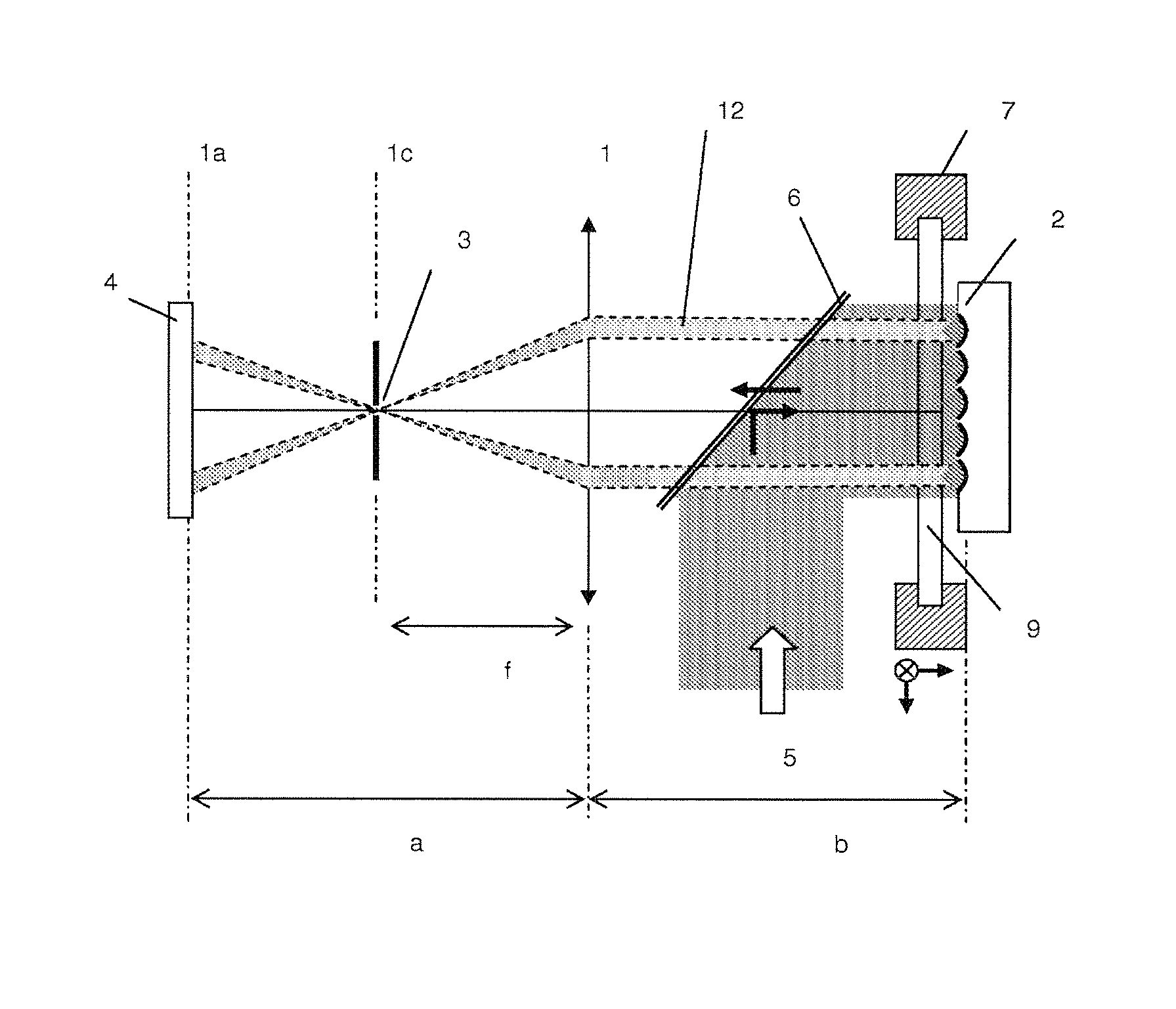
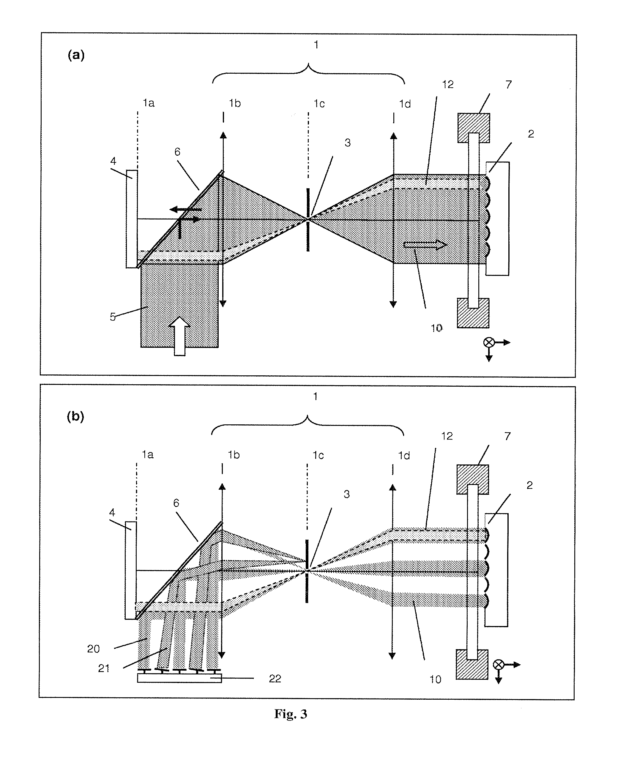
[0045]Confocal scanning microscopy is a nowadays widely used technique, whether it is for biological or micromanufacturing applications. Since resolution is now brought down the micron, high NA is a requirement and mirrors have the potential to provide it while operating in array format. They can notably improve some of the actual systems limitations. One is the field of view limitation of most confocal microscopes that appears to use beam scanning within a high NA objective. The scan is indeed done within the field of view of the objective, rather small if providing high NA. A single focusing mirror would not overstep this limitation but the present invention proposes to use micromirrors arranged in a two dimensional array in order to perform simultaneous multi-confocal detection for large-field imaging.

[0046]Besides, the increasing development of microsystems, particularly for biological and chemical applications, encourages th...


PUM


Abstract

The invention relates to large-field high-resolution microscopy and photolithography setups operating with polychromatic light. It includes the use of a plurality of focusing micromirrors.

Description

[0001]This application is the U.S. national phase of International Application No. PCT / IB2010 / 050300, filed 23 Jan. 2010, which designated the U.S., and claims priority to IB Application No. PCT / IB2009 / 050285, filed 24 Jan. 2009, the entire contents of each of which are hereby incorporated by reference.FIELD OF INVENTION[0002]The present invention generally relates to high-resolution microscopy and microlithography. Its primary aimed application in the high-resolution microscopy domain would be parallel scanning confocal microscopy, with special emphasis on polychromatic light applications. The primary aimed application in the high-resolution microlithography domain is parallel micro- and nano-structuring based on two-photon polymerization with ultra-short pulsed lasers.[0003]The following description will mainly focus on confocal microscopy, with a few variants of the system presented for demonstrating the versatility of the invention. However, it is understood that the invention c...

Claims


Application Information

Patent Timeline
Patent Type & Authority Patents(United States)
IPC IPC(8): G02B21/00
CPCG02B21/004G02B21/0032G02B21/0076G02B26/0833G03F7/70191
Inventor RACHET, BASTIENMERENDA, FABRICESALATHE, RENE
Owner ECOLE POLYTECHNIQUE FEDERALE DE LAUSANNE (EPFL)
Learn More