Fabrication method for high-density MRAM using thin hard mask
a fabrication method and high-density technology, applied in the direction of electrical equipment, galvano-magnetic device manufacture/treatment, and semiconductor devices, can solve the problems of loss of magnetic properties, degrade and damage the magnetic properties, and the conventional method of mtj etching is reaching its limit in process capability, so as to increase the incident ibe angle
- Summary
- Abstract
- Description
- Claims
- Application Information
AI Technical Summary
Benefits of technology
Problems solved by technology
Method used
Image
Examples
first embodiment
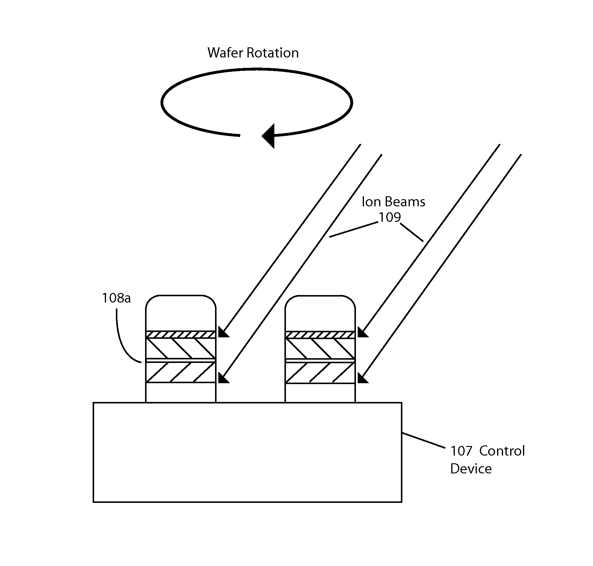
[0030]FIGS. 3 to 12 will be used to describe the first embodiment of the invention. FIG. 3 illustrates a selected stage of the MTJ and hard mask deposition process. The hard mask in the first embodiment is a single layer film, but in the second embodiment described below the hard mask includes two layers. As shown in FIG. 3 the MTJ layers have been deposited on the previously patterned control device 107 which is formed using standard techniques and is not described in this disclosure. The multiple layers in the stack for the MRAM cells have been deposited in sequence over the control device 107. The lowest layer in the cell is the bottom electrode (BE) layer 106, which is followed by the multiple layers in the MTJ stack which includes conventional layers such as the free and pinned magnetic layers and the barrier layer 104. Because the magnetic free layer, for example, can be the upper magnetic layer 103 or the lower magnetic layer 105 according to standard MTJ principles, the foll...
second embodiment
[0039]FIGS. 13 to 15 illustrate the second embodiment of the invention. In this embodiment bi-layer hard mask films are used instead of single hard mask film compared to the first embodiment. The upper layer in the bi-layer hard mask structure is totally removed during processing, but the lower layer becomes the top electrode pads. FIG. 13 illustrates that the MTJ is deposited on the control device 207 which is not described herein. The multiple layers in the stack for the MRAM cell have been deposited in sequence over the control device 207. The lowest layer in the cell is the bottom electrode (BE) layer 206, which is followed by the MTJ stack deposition in the sequence of bottom magnetic layer 205, tunnel barrier layer 204 and top magnetic layer 203. The MTJ is covered with capping layer 202, which should be a metallic material which has some selectivity during hard mask bi-layer etching. The hard mask is preferably ruthenium; therefore, Ta, Ti, TiN, TaN, W, WN, Cr, and Al are pos...
PUM
| Property | Measurement | Unit |
|---|---|---|
| size | aaaaa | aaaaa |
| thickness | aaaaa | aaaaa |
| thickness | aaaaa | aaaaa |
Abstract
Description
Claims
Application Information
 - R&D
- Intellectual Property
- Life Sciences
- Materials
- Tech Scout
- Unparalleled Data Quality
- Higher Quality Content
- 60% Fewer Hallucinations
Browse by: Latest US Patents, China's latest patents, Technical Efficacy Thesaurus, Application Domain, Technology Topic, Popular Technical Reports.
© 2025 PatSnap. All rights reserved.Legal|Privacy policy|Modern Slavery Act Transparency Statement|Sitemap|About US| Contact US: help@patsnap.com


