Rolled copper or copper-alloy foil provided with roughened surface
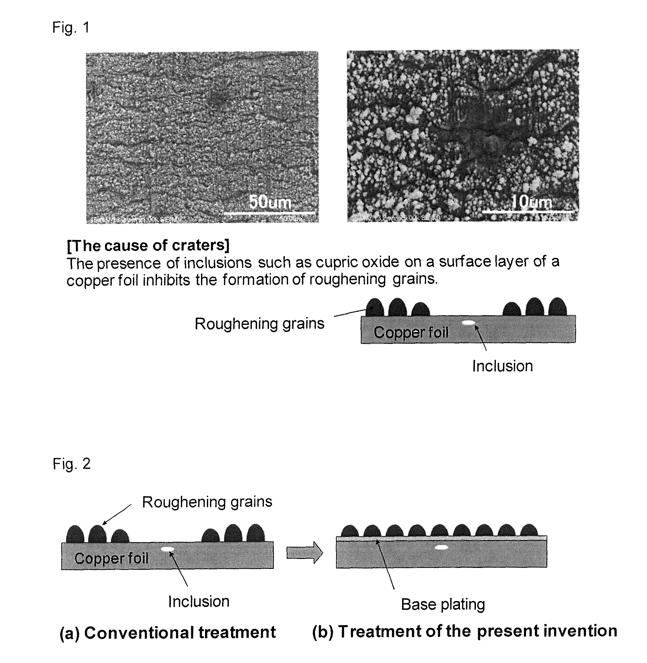
a technology of rolled copper or copper alloy foil and roughened surface, which is applied in the direction of enhancing the adhesion of the metal to the insulation substrate, transportation and packaging, and chemistry apparatus and processes, etc., can solve the problem of insufficient fine pattern formation, difficulty in etching at a high aspect ratio, and occurrence of undercutting upon etching, etc. problem, to achieve good adhesive strength, inhibit the development of craters, and high strength
- Summary
- Abstract
- Description
- Claims
- Application Information
AI Technical Summary
Benefits of technology
Problems solved by technology
Method used
Image
Examples
example 1
[0065]A rolled copper alloy foil comprising Cr: 0.2 wt %, Zr: 0.1 wt %, Zn: 0.2 wt %, and the remainder being Cu and unavoidable impurities was used as a copper foil.
[0066]This rolled copper foil was degreased and then washed with water, and subsequently washed with acid and then water, and then a copper base plating layer having a thickness of 0.04 μm was formed under the following conditions: copper sulfate (Cu equivalence: 20 g / L), sulfuric acid: 100 g / L, temperature: 50° C., and Dk: 5.0 A / dm2 (C: 10.3 As / dm2). The thickness of a base plating layer is a theoretical value from the amount of coulomb and the specific gravity of copper.
[0067]Next, roughening treatment via copper plating with 0.4 μm copper grains was further performed on the base plating layer under the condition of Dk: 50 A / dm2 (C: 70 As / dm2).
[0068]For this rolled copper-alloy foil subjected to the roughening plating, various evaluation tests were conducted under the conditions set forth in the followings. Note that ...
example 2
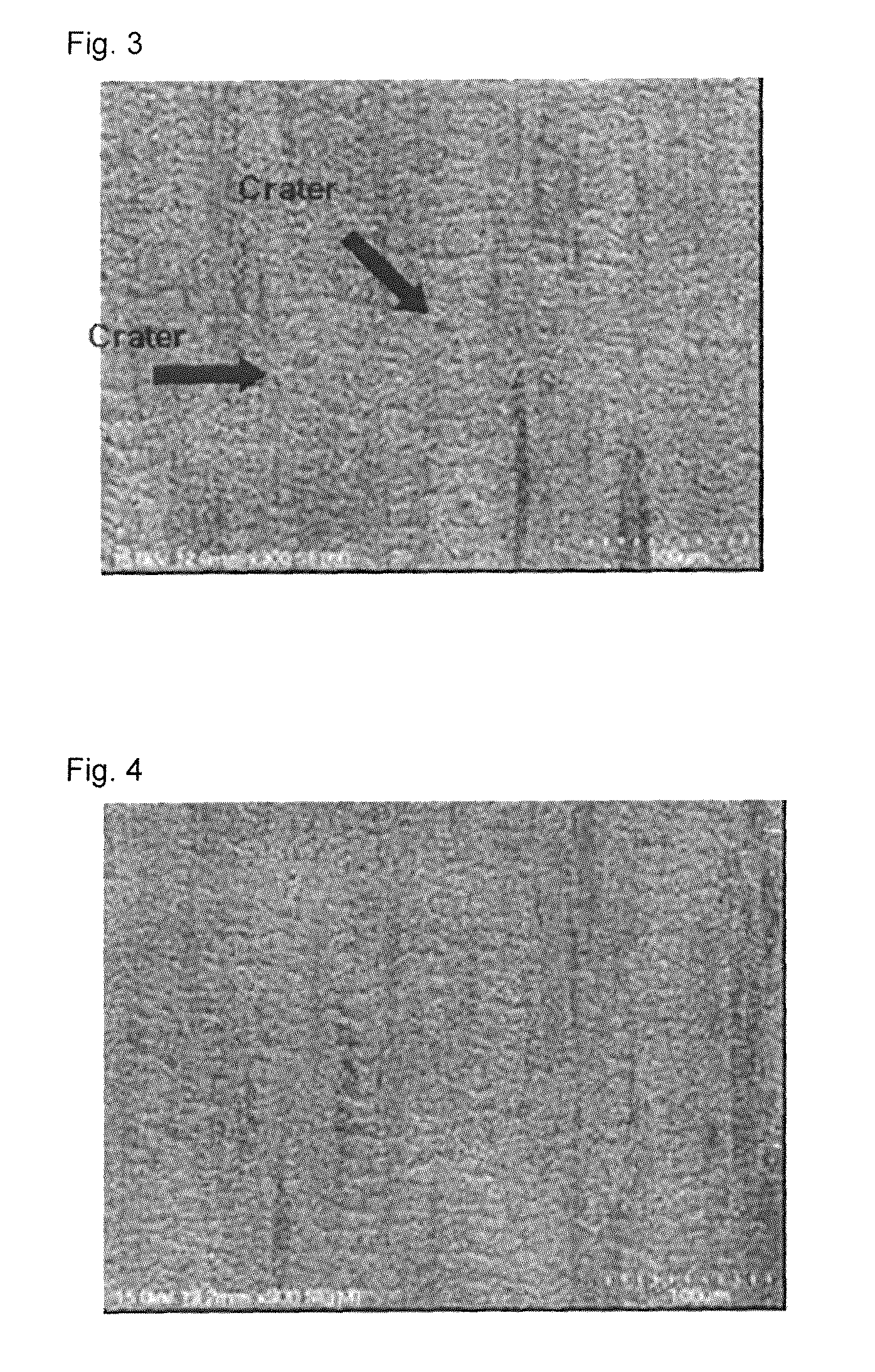
[0073]A copper base plating layer with a thickness of 0.08 μm was formed under the condition for forming a copper base plating layer of Dk: 10.0 A / dm2 (C: 20.7 As / dm2). Other conditions are the same as in Example 1. The number of craters on the copper roughened surface was counted under a light microscope to investigate the number. The results are also shown in Table 1. As shown in Table 1, Example 2 showed fewer craters, and the number was 2.1 per 25 mm2.
example 3
[0074]A copper base plating layer with a thickness of 0.15 μm was formed under the condition for forming a copper base plating layer of Dk: 15.0 A / dm2 (C: 41.0 As / dm2). Other conditions are the same as in Example 1. The number of craters on the copper roughened surface was counted under a light microscope to investigate the number. The results are also shown in Table 1. As shown in Table 1, Example 3 showed fewer craters, and the number was 0.5 per 25 mm2.
PUM
| Property | Measurement | Unit |
|---|---|---|
| thickness | aaaaa | aaaaa |
| size | aaaaa | aaaaa |
| size | aaaaa | aaaaa |
Abstract
Description
Claims
Application Information
 - R&D
- Intellectual Property
- Life Sciences
- Materials
- Tech Scout
- Unparalleled Data Quality
- Higher Quality Content
- 60% Fewer Hallucinations
Browse by: Latest US Patents, China's latest patents, Technical Efficacy Thesaurus, Application Domain, Technology Topic, Popular Technical Reports.
© 2025 PatSnap. All rights reserved.Legal|Privacy policy|Modern Slavery Act Transparency Statement|Sitemap|About US| Contact US: help@patsnap.com


