
Semiconductor device with corner tie bars

a technology of semiconductor devices and lead frames, applied in semiconductor devices, semiconductor/solid-state device details, electrical apparatus, etc., can solve the problems of increasing the number of exposed electrical contacts of the device, short circuit between two bond wires, and excessive or variable mutual inductan

Active Publication Date: 2015-04-07
NXP USA INC
View PDF5 Cites 6 Cited by
  • Summary
  • Abstract
  • Description
  • Claims
  • Application Information

AI Technical Summary

Benefits of technology

The present invention relates to a semiconductor device assembly and, more particularly, to a lead frame with corner tie bars used in the assembly process. The invention aims to address the problem of wire sweep, which can result in excessive proximity of adjacent bond wires, leading to short circuits and variable mutual inductance. The invention provides a solution to reduce the effects of wire sweep and ensure more exposed electrical contacts while also reducing the size of semiconductor devices and the spacing between the bond wires.

Problems solved by technology

Such movement can result in excessive proximity of adjacent bond wires, resulting in excessive or variable mutual inductance, or even short circuits between two bond wires.
Continued reduction in the size of semiconductor devices and increases in their complexity results in an increase in the number of exposed electrical contacts of the devices and a reduction in the spacing between the electrical contacts and the spacing between the bond wires.

Method used


Image

  • Semiconductor device with corner tie bars
  • Semiconductor device with corner tie bars
  • Semiconductor device with corner tie bars

Examples


Embodiment Construction

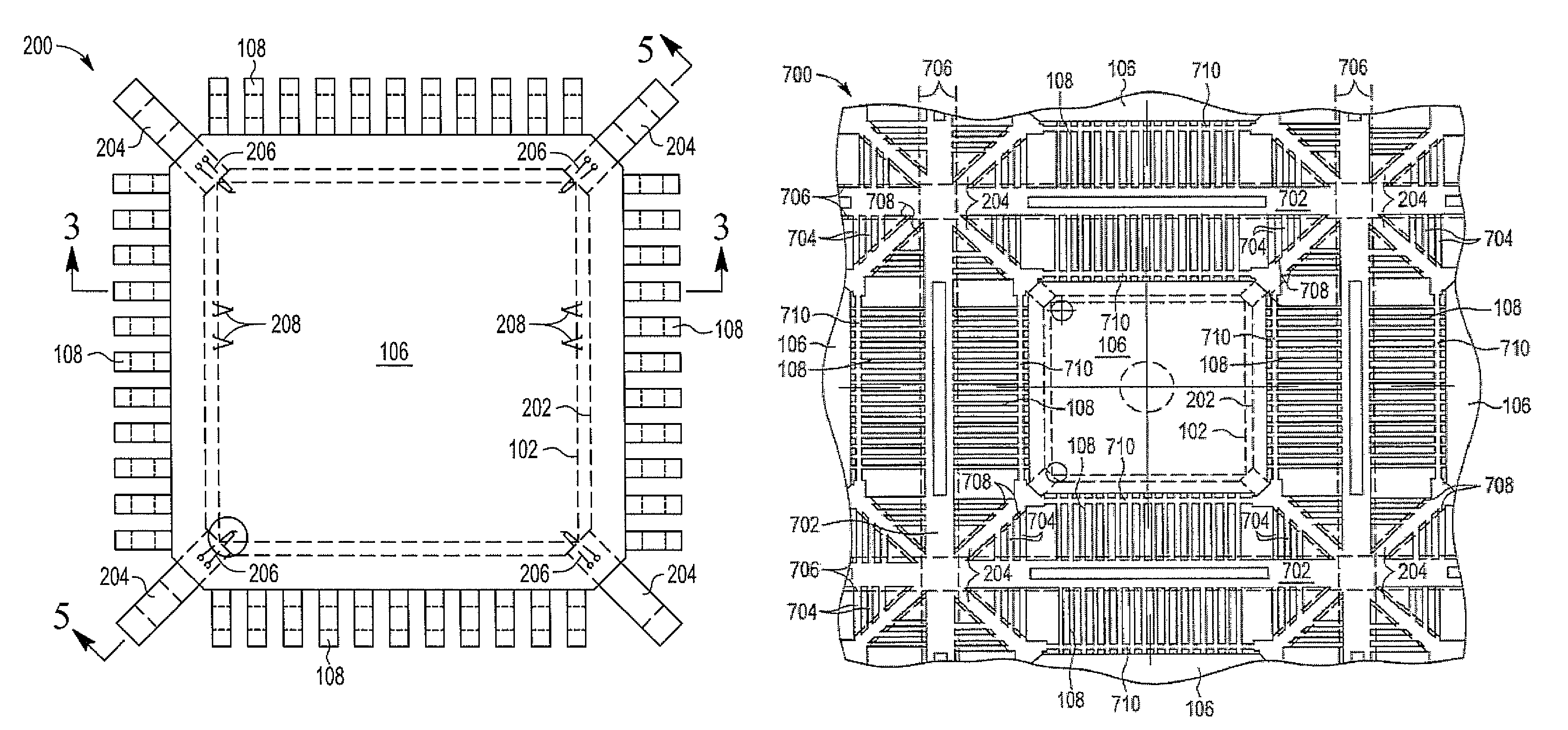
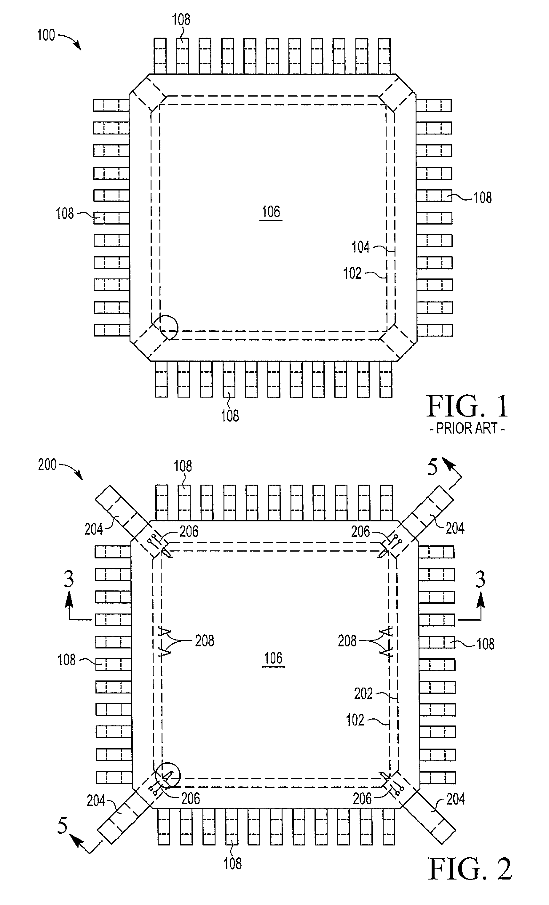
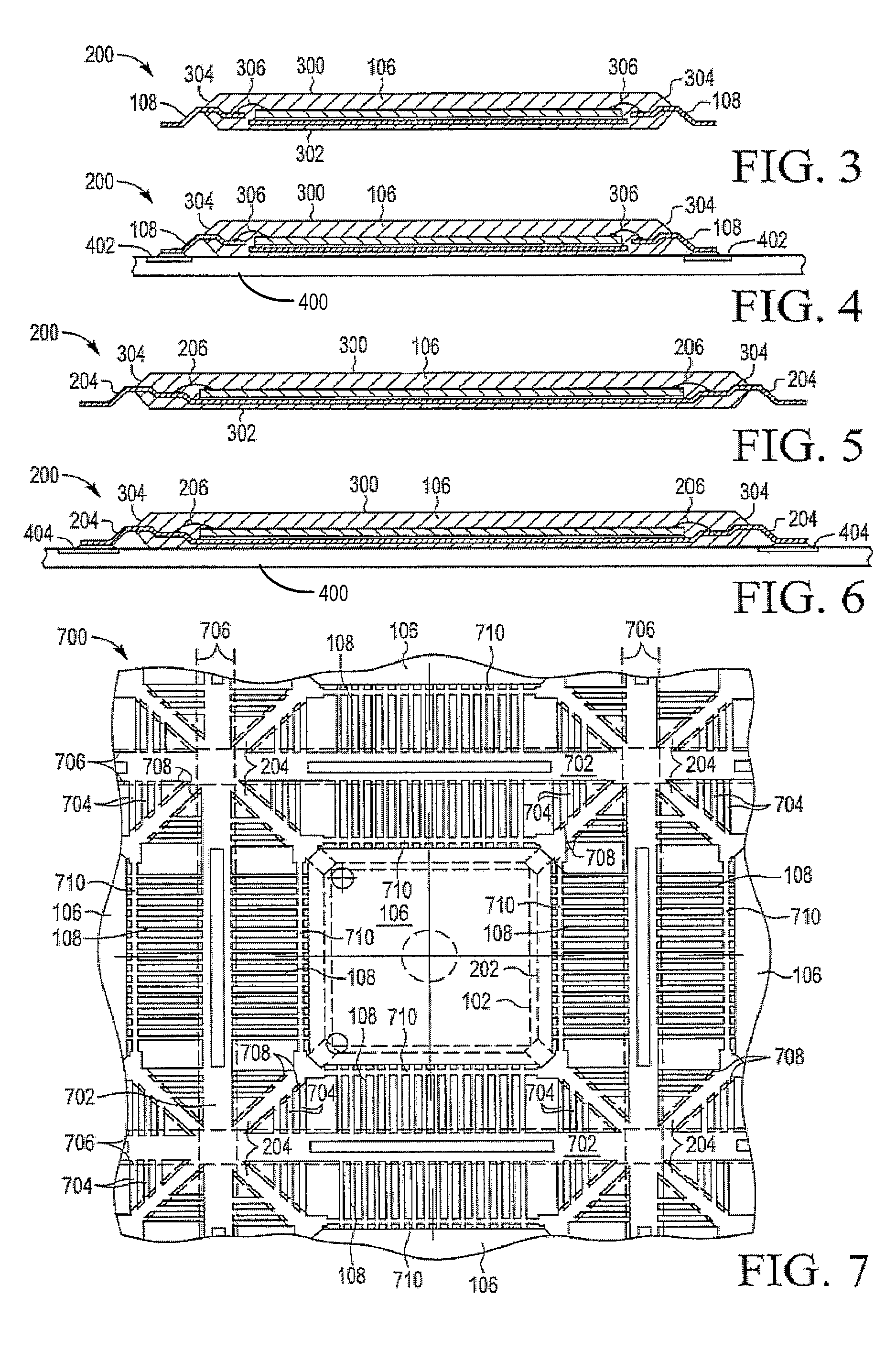
[0017]FIG. 1 illustrates a conventional quad flat package (QFP) semiconductor device 100. The semiconductor device 100 comprises one or more semiconductor dies 102 mounted on an electrically and thermally conductive flag (or die pad or paddle) 104. The die 102 and the flag 104 are embedded in a molding compound or encapsulation 106 having top and bottom faces and an edge surface. The die 102 and flag 104 are shown in dashed lines. A set of exposed electrical leads 108 are connected with internal electrical contacts (not shown) on an active face of the die 102, the electrical leads 108 being supported by the encapsulation 106 and projecting from the edge surface for connection to an external electrical circuit.

[0018]The semiconductor device 100 is of the non-exposed pad type, in which the flag 104 is embedded in the encapsulation 106 and is not exposed in the bottom face of the encapsulation 106. Accordingly, power ground connections cannot be made directly to the flag 104 and one or...


PUM


Abstract

A Quad Flat Pack (QFP) type semiconductor device includes four corner tie bars that, instead of being trimmed, are used for power and / or ground connections, and alternatively, to control mold flow during the encapsulation step of the assembly process.

Description

BACKGROUND OF THE INVENTION[0001]The present invention is directed to semiconductor device assembly and, more particularly, to a lead frame with corner tie bars used in the assembly process.[0002]Semiconductor device packaging fulfills basic functions such as providing electric connections and protecting the die against mechanical and environmental stresses. An assembled semiconductor device has exposed electrical contacts and may be mounted on a support, such as a printed circuit board (PCB), for example, where the exposed electrical contacts are connected to external electronic circuits on the support. Using surface mount technology, the exposed electrical contacts of the device can be soldered directly to corresponding electrical contact pads on the support, providing mechanical attachment as well as electrical connections.[0003]Semiconductor devices are commonly packaged for surface mounting by encapsulating one or more semiconductor dies in a mold compound. The encapsulation pr...

Claims


Application Information

Patent Timeline
Patent Type & Authority Patents(United States)
IPC IPC(8): H01L23/495H01L21/82
CPCH01L23/49575H01L21/82H01L23/49541H01L23/49551H01L23/3107H01L24/97H01L2224/32245H01L2224/48091H01L2224/48247H01L2224/73265H01L2924/181H01L2224/97H01L2924/00014H01L2924/00
Inventor CHAN, WENG HOONGKHOO, LY HOONLOW, BOON YEW
Owner NXP USA INC
Learn More