Touch panel and fabrication method thereof
a technology of touch panel and fabrication method, which is applied in the field of touch panel and a fabrication method thereof, can solve the problems of affecting the manufacturing yield rate, well alleviated, and deterioration of the reliability of the substrate, and achieve the effect of favorable reliability
- Summary
- Abstract
- Description
- Claims
- Application Information
AI Technical Summary
Benefits of technology
Problems solved by technology
Method used
Image
Examples
first embodiment
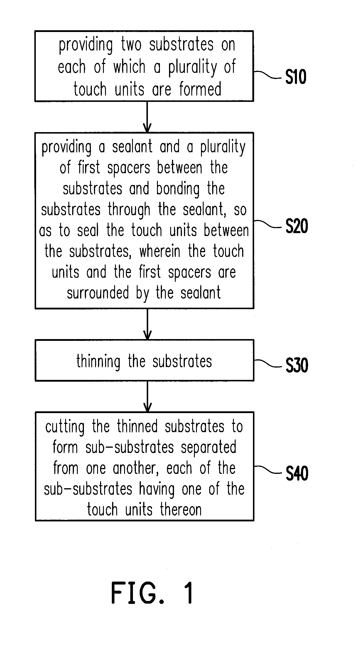
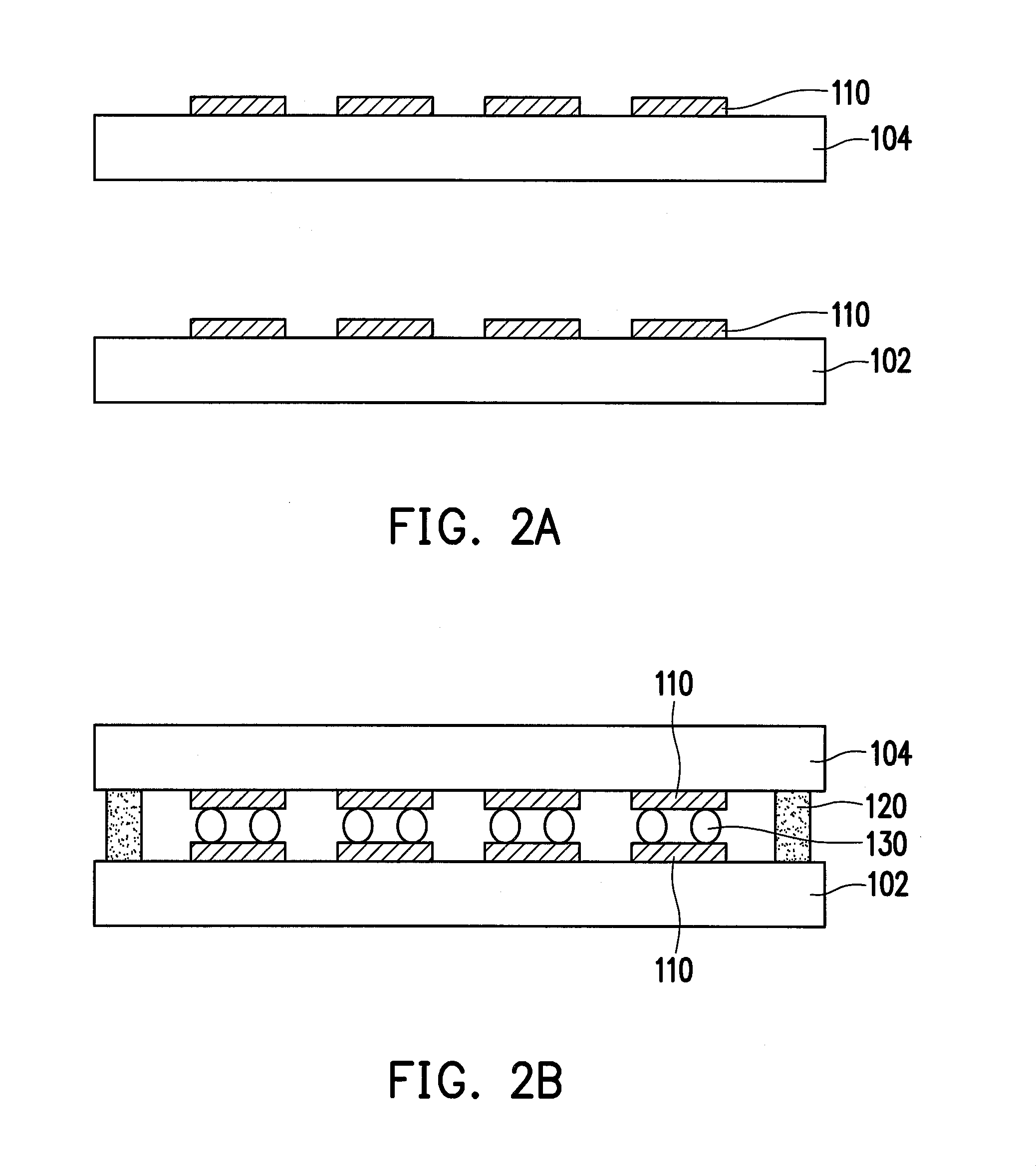
[0031]FIG. 1 is a flow chart illustrating a fabrication method of a touch panel according to an embodiment of the invention. FIG. 2A to FIG. 2E are schematic views illustrating a fabrication method of a touch panel according to a first embodiment of the invention. With reference to FIG. 1 and FIG. 2A, in step S10, two substrates 102 and 104 are provided, and a plurality of touch units 110 are already formed on each of the substrates 102 and 104. In this embodiment, the substrates 102 and 104 are, for instance, glass substrates, quartz substrates, or other appropriate substrates. Each of the touch units 110 is a capacitive touch circuit layer, for instance. Specifically, in this embodiment, each of the touch units 110 includes a plurality of first sensing series (not shown) extending along a first direction and a plurality of second sensing series (not shown) extending along a second direction, for instance. Each of the first sensing series has a plurality of first electrodes seriall...
second embodiment
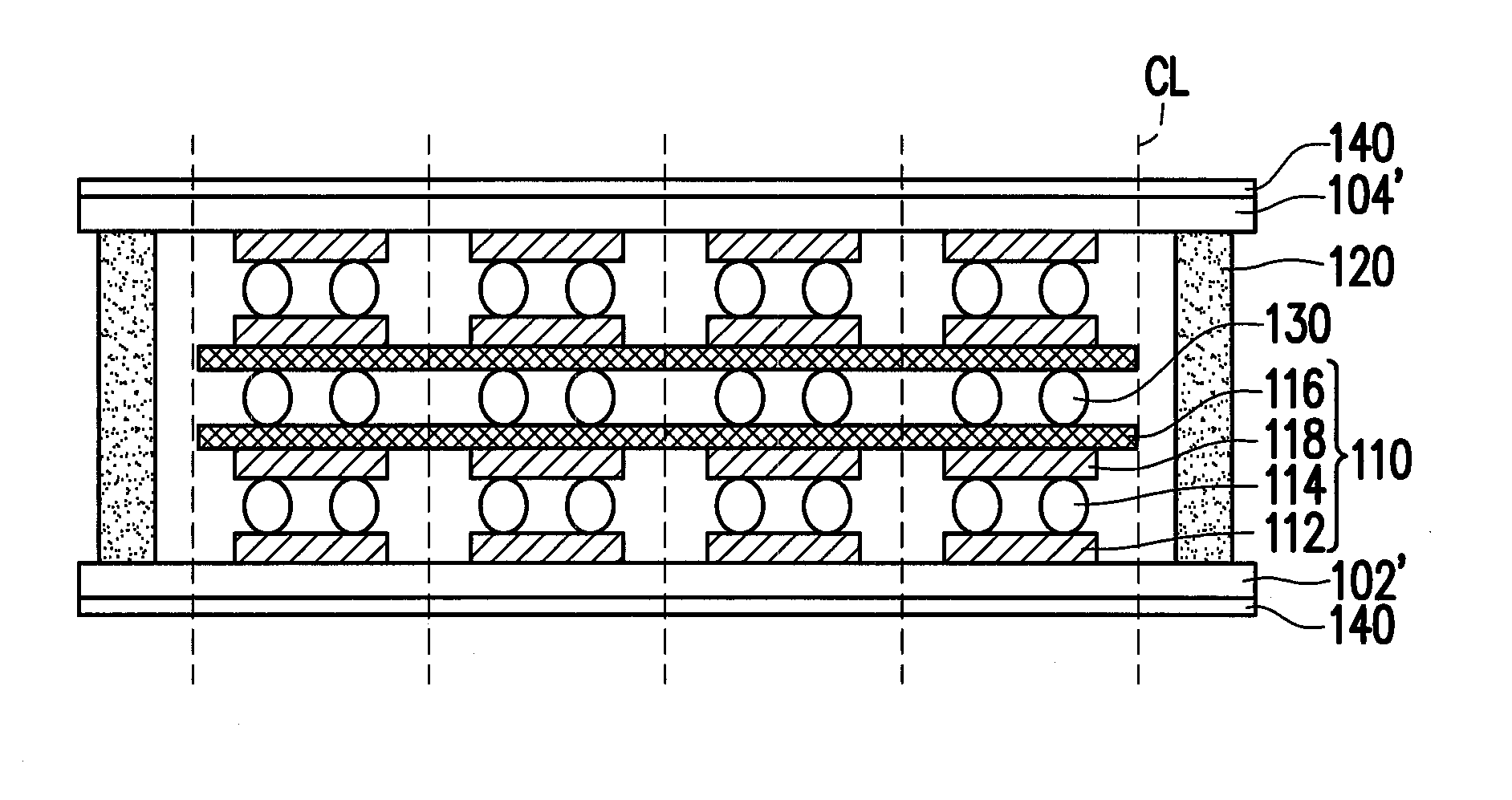
[0038]FIG. 4A to FIG. 4E are schematic views illustrating a fabrication method of a touch panel according to a second embodiment of the invention. With reference to FIG. 1 and FIG. 4A, in step S10, two substrates 102 and 104 on each of which a plurality of touch units 110 are formed are provided. In this embodiment, each of the touch units 110 is a resistant touch circuit layer, for instance. To be more specific, in this embodiment, each of the touch units 110 is formed by forming a plurality of first patterned circuit layers 112 on each of the substrates 102 and 104 and then forming a plurality of second spacers 114 on each of the first patterned circuit layers 112. A plurality of carriers 116 are provided. The carriers 116 include but are not limited to flexible thin films or plastic substrate materials, and a second patterned circuit layer 118 is already formed on each of the carriers 116. Each of the carriers 116 is bonded to the substrate 102 or the substrate 104 to cover one o...
third embodiment
[0044]FIG. 5A to FIG. 5F are schematic views illustrating a fabrication method of a touch panel according to a third embodiment of the invention. With reference to FIG. 1 and FIG. 5A, in step S10, two substrates 102 and 104 on each of which a plurality of touch units 110 are formed are provided. In this embodiment, each of the touch units 110 is a resistant touch circuit layer, for instance, and each of the touch units 110 is formed by forming a plurality of first patterned circuit layers 112 on each of the substrates 102 and 104, for instance.
[0045]With reference to FIG. 1 and FIG. 5B, in step S20, a sealant 120 and a plurality of first spacers 130 are provided between the substrates 102 and 104, and the substrates 102 and 104 are bonded together through the sealant 120, such that the touch units 110 are sealed between the substrates 102 and 104. Here, the touch units 110 and the first spacers 130 are surrounded by the sealant 120. In this embodiment, the method of forming the firs...
PUM
| Property | Measurement | Unit |
|---|---|---|
| electromagnetic-wave | aaaaa | aaaaa |
| electromagnetic-wave shielding | aaaaa | aaaaa |
| weight | aaaaa | aaaaa |
Abstract
Description
Claims
Application Information
 - R&D
- Intellectual Property
- Life Sciences
- Materials
- Tech Scout
- Unparalleled Data Quality
- Higher Quality Content
- 60% Fewer Hallucinations
Browse by: Latest US Patents, China's latest patents, Technical Efficacy Thesaurus, Application Domain, Technology Topic, Popular Technical Reports.
© 2025 PatSnap. All rights reserved.Legal|Privacy policy|Modern Slavery Act Transparency Statement|Sitemap|About US| Contact US: help@patsnap.com


