Electrophoretic display device, electronic apparatus, and method of driving electrophoretic display device

a display device and electrophoretic technology, applied in the direction of instruments, static indicating devices, etc., can solve the problems of organic transistors noticeably having a characteristic degradation problem, the contrast of electrophoretic display devices is reduced, etc., and the display quality of electrophoretic display devices may be maintained.

Active Publication Date: 2015-01-06
E INK CORPORATION
View PDF8 Cites 8 Cited by
  • Summary
  • Abstract
  • Description
  • Claims
  • Application Information

AI Technical Summary

Benefits of technology

[0008]An advantage of some aspects of the invention is that it suppresses degradation of characteristic of a transistor used as a switching element, and maintains the display quality of the electrophoretic display device.

Problems solved by technology

This results in a decrease in contrast of the electrophoretic display device or may produce a problem such as nonoperation of the electrophoretic display device in some cases.
Particularly, the organic transistor noticeably has a problem of characteristic degradation due to the carrier trap.

Method used


Image

  • Electrophoretic display device, electronic apparatus, and method of driving electrophoretic display device
  • Electrophoretic display device, electronic apparatus, and method of driving electrophoretic display device
  • Electrophoretic display device, electronic apparatus, and method of driving electrophoretic display device

Examples


first embodiment

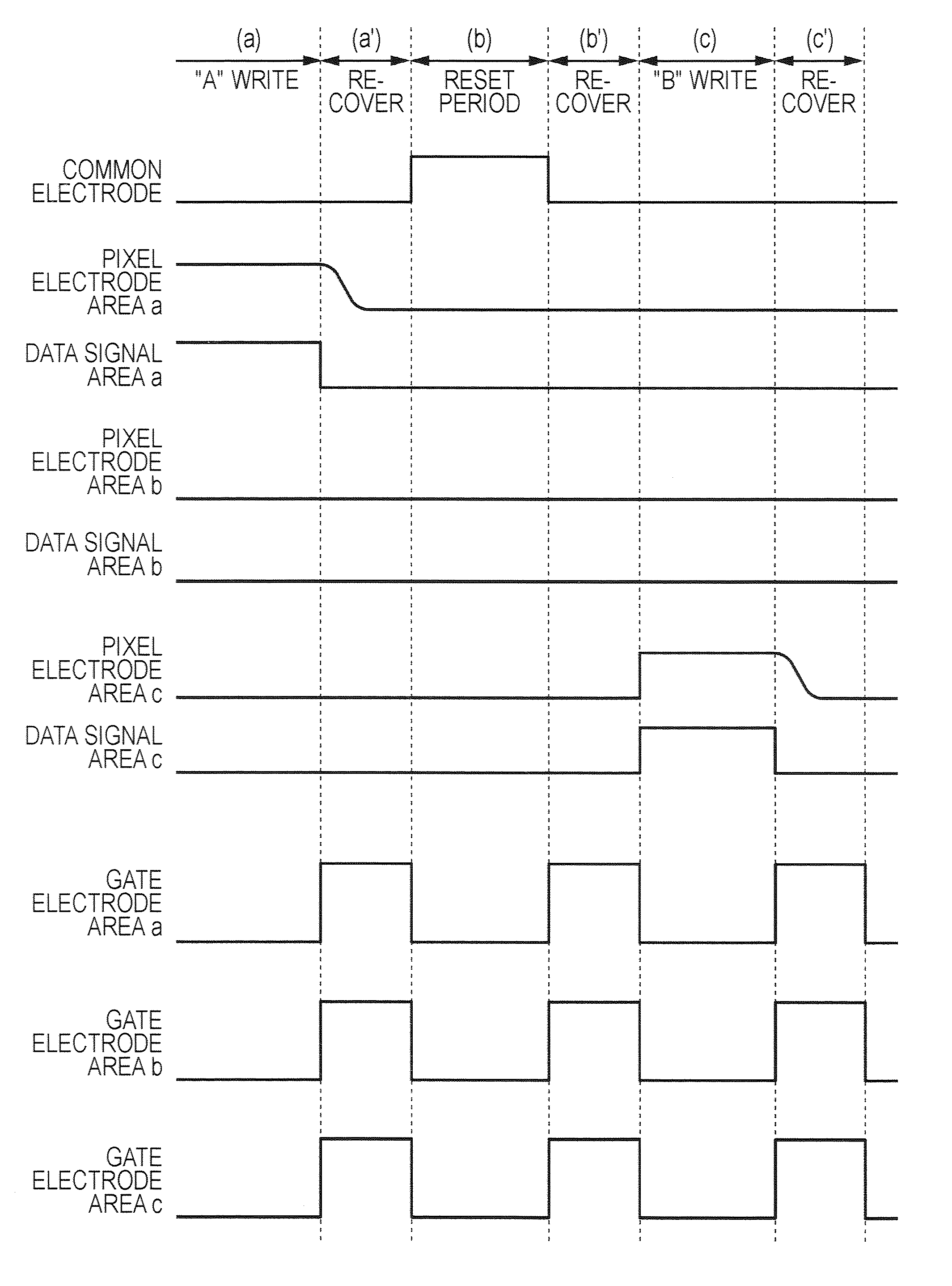
[0033]FIG. 1 is a view that shows a general electrical configuration of an electrophoretic display device 10 according to a first embodiment. An electrophoretic display panel A (display portion) is formed of a plurality of pixels. Each of the pixels includes a TFT 103, which serves as a switching element described later, and a pixel electrode 104 connected to the TFT 103. On the other hand, a scanning line driving circuit 130 and a data line driving circuit 140 are formed in a peripheral area of a device substrate 100. In addition, a plurality of scanning lines 101 are formed on the electrophoretic display panel A of the device substrate 100 so as to be parallel to an X direction shown in the drawing. In addition, a plurality of data lines 102 are formed so as to be parallel to a Y direction that is perpendicular to the X direction. Then, pixels are arranged in a matrix at positions corresponding to intersections of the scanning lines 101 and the data lines 102.

[0034]A controller (c...


PUM


Abstract

An electrophoretic display device includes a common electrode, pixel electrodes, and a disperse system of electrophoretic particles. A transistor supplies one of the pixel electrodes with a first potential or a second potential higher than the first potential. During a first period, a control portion supplies a third potential to the gate electrode to turn on the transistor, supplies the first potential to a signal line or the common electrode, and supplies the second potential to the other line. During a second period, the control portion supplies a fourth potential higher than the third potential to the gate electrode to turn off the transistor, and supplies the first potential to both the signal line and the common electrode so that the pixel electrode potential substantially reaches the common electrode potential. The third potential is lower than the second potential and the fourth potential is higher than the first potential.

Description

BACKGROUND[0001]1. Technical Field[0002]The present invention relates to an electrophoretic display device, an electronic apparatus, and a method of driving an electrophoretic display device.[0003]2. Related Art[0004]An electrophoretic display device is formed so that electrophoretic fluid dispersion that includes one or more types of electrophoretic particles and an electrophoretic dispersion medium is sealed between a pair of opposite electrode plates, at least one of which is transparent. Applying a voltage between the two electrodes causes electrophoretic particles to move in the electrophoretic dispersion medium, and a change in dispersion of the electrophoretic particles varies optical reflection property to thereby make it possible to display information. At this time, if one of the electrodes is formed of a plurality of divided pixel electrodes, by controlling an electric potential of each pixel electrode, a difference in dispersion of particles in each pixel is produced to ...

Claims


Application Information

Patent Timeline
Patent Type & Authority Patents(United States)
IPC IPC(8): G09G3/34
CPCG09G3/344G09G2300/0842G09G2300/0876G09G2310/063
Inventor MORIYA, SOICHIMIYAMOTO, TSUTOMU
Owner E INK CORPORATION
Why Eureka
Try Eureka