Manufacturing method for layered chip packages

a manufacturing method and chip technology, applied in the direction of electrical equipment, semiconductor devices, semiconductor/solid-state device testing/measurement, etc., can solve the problems of failure of the chip to operate normally, the conformance of the chip included in the layered chip package is lower than the yield of the chip, and the chip including the control circuit and a plurality of memory cells becomes defective, etc., to achieve the effect of easy manufacturing and low cos

Inactive Publication Date: 2014-12-16
HEADWAY TECH INC +1
View PDF10 Cites 0 Cited by
  • Summary
  • Abstract
  • Description
  • Claims
  • Application Information

AI Technical Summary

Benefits of technology

[0009]It is an object of the present invention to provide a manufacturing method for a plurality of layered chip packages that makes it possible to manufacture easily and at low cost a plurality of layered chip packages each of which includes a plurality of stacked semiconductor chips and is capable of providing, even if a defective semiconductor chip is included therein, the same functions as those for the case where no defective semiconductor chip is included.
[0020]According to the manufacturing method for the layered chip packages of the present invention, the layered substructure with at least one additional package joined thereto is used to produce a plurality of layered chip packages. The present invention thus makes it possible to manufacture layered chip packages easily and at low cost, each of the layered chip packages including a plurality of stacked semiconductor chips and being capable of providing, even if a defective semiconductor chip is included therein, the same functions as those for the case where no defective semiconductor chip is included.

Problems solved by technology

Therefore, the possibility that all the chips included in a layered chip package are conforming is lower than the yield of the chips.
Suppose, however, that a chip including a control circuit and a plurality of memory cells becomes defective due to, for example, a wiring failure in the control circuit, and even the redundancy technique cannot allow the chip to operate normally.
In such a case, the defective chip is no longer usable.
However, this increases the manufacturing cost of the layered chip package.
This technology, however, has room for improvement in terms of simplification of the manufacturing process and in terms of manufacturing cost.

Method used


Image

  • Manufacturing method for layered chip packages
  • Manufacturing method for layered chip packages
  • Manufacturing method for layered chip packages

Examples


first embodiment

[0085]Preferred embodiments of the present invention will now be described in detail with reference to the drawings. A manufacturing method according to a first embodiment of the invention is a method for manufacturing a plurality of layered chip packages. Each of the plurality of layered chip packages manufactured by the manufacturing method according to the present embodiment includes a main package. At least one of the plurality of layered chip packages is a composite layered chip package which further includes an additional package stacked on the main package.

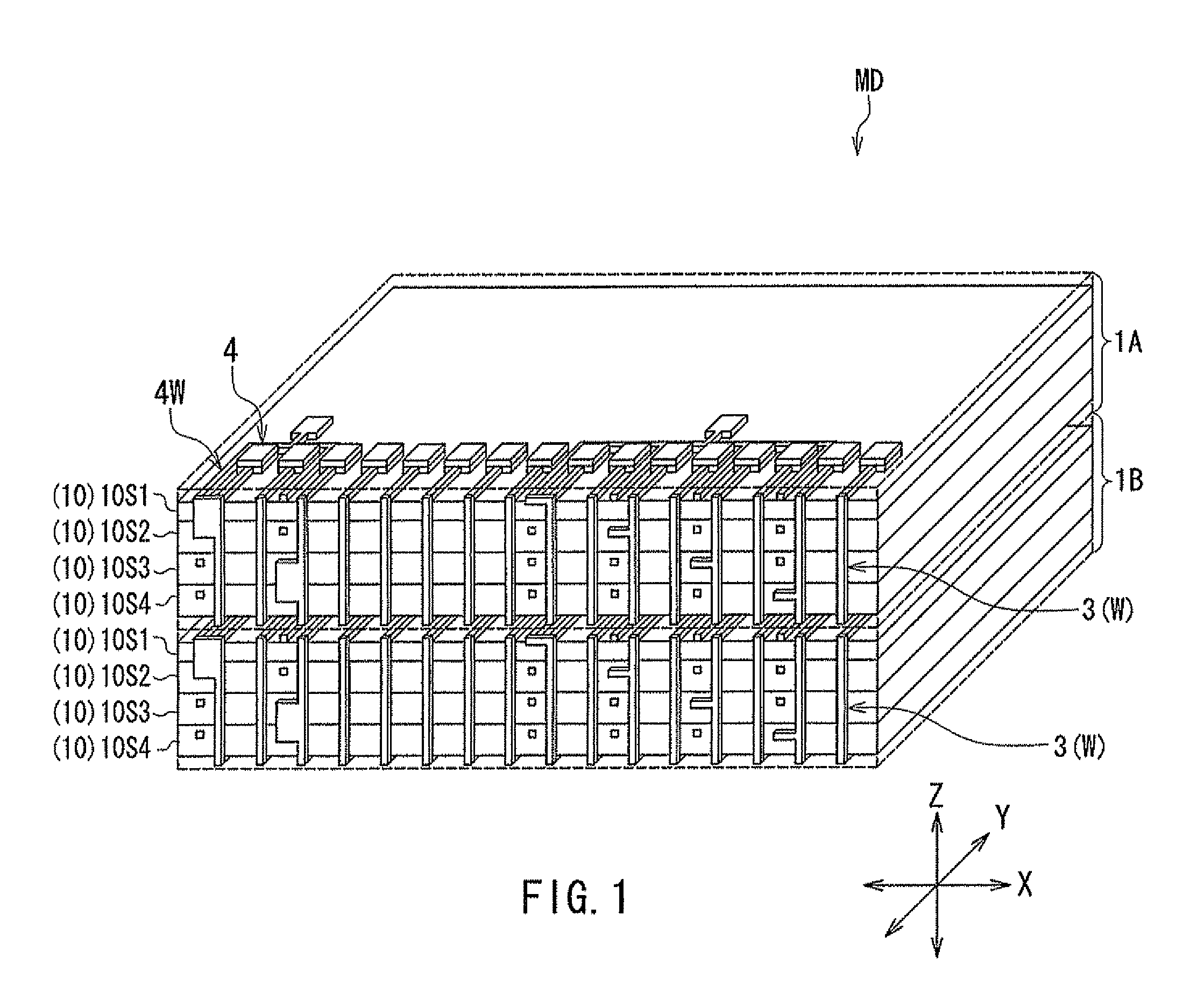
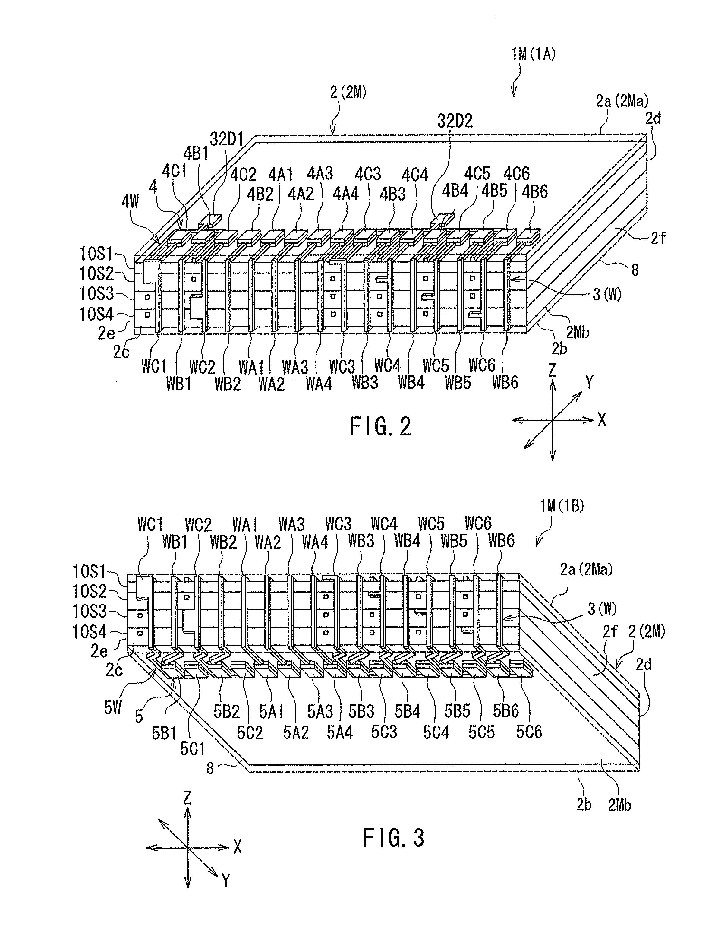
[0086]First, reference is made to FIG. 1 to FIG. 6 to describe the configuration of the main package of the present embodiment. FIG. 1 is a perspective view of a module including two main packages of the present embodiment. FIG. 2 is a perspective view of a main package of the present embodiment. FIG. 3 is a perspective view showing the main package of FIG. 2 as viewed from below. FIG. 4 is a plan view showing a layer porti...

second embodiment

[0252]A second embodiment of the invention will now be described. First, reference is made to FIG. 42 to FIG. 47 to describe the configuration of the main package of the present embodiment. FIG. 42 is a perspective view of a module including four main packages of the present embodiment. FIG. 43 is a perspective view of a single main package of the present embodiment. FIG. 44 is a perspective view showing the main package of FIG. 43 as viewed from below. FIG. 45 is a plan view showing a layer portion included in the main package of FIG. 43. FIG. 46 is a perspective view of the layer portion shown in FIG. 45. FIG. 47 is a plan view showing a plurality of bottom terminals and bottom wiring of the main package of FIG. 43 as viewed from above.

[0253]The module MD shown in FIG. 42 includes four main packages 1C, 1D, 1E, and 1F that are stacked and electrically connected to each other. The main packages 1C, 1D, 1E, and 1F are arranged in this order from the top. In the following description...

third embodiment

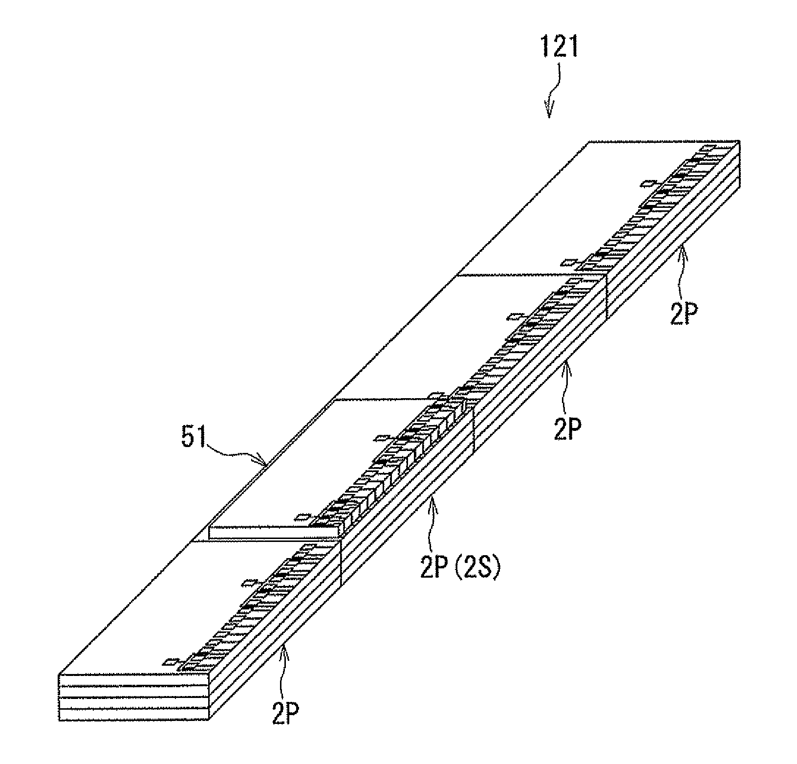
[0317]A third embodiment of the invention will now be described. The present embodiment differs from the second embodiment in the configuration of the additional package and the relative positional relationship between the main package and the additional package in the composite layered chip package 1.

[0318]The additional package will now be described with reference to FIG. 56 to FIG. 59. FIG. 56 is a perspective view of the additional package. FIG. 57 is a perspective view showing the additional package of FIG. 56 as viewed from below. FIG. 58 is a plan view of the additional package of FIG. 56. FIG. 59 is a plan view showing the plurality of bottom terminals and the bottom wiring of the additional package of FIG. 56 as viewed from above.

[0319]The configuration of the additional package 51 of the present embodiment is the same, as that of the additional package 51 of the second embodiment except for the configuration of the plurality of bottom terminals 55, the plurality of conduct...


PUM


Abstract

In a manufacturing method for layered chip packages, a layered substructure with at least one additional package joined thereto is used to produce a plurality of layered chip packages. The layered substructure includes a plurality of main bodies to be separated from each other later. Each main body includes: a main part having top and bottom surfaces and including a plurality of layer portions stacked on each other; and a plurality of main terminals disposed on at least one of the top and bottom surfaces of the main part. The additional package includes an additional semiconductor chip and at least one additional terminal that is electrically connected to the additional semiconductor chip and in contact with at least one of the plurality of main terminals.

Description

BACKGROUND OF THE INVENTION[0001]1. Field of the Invention[0002]The present invention relates to a manufacturing method for layered chip packages each of which includes a plurality of stacked semiconductor chips.[0003]2. Description of the Related Art[0004]In recent years, lighter weight and higher performance have been demanded of portable devices typified by cellular phones and notebook personal computers. Accordingly, there has been a need for higher integration of electronic components for use in the portable devices. With the development of image- and video-related equipment such as digital cameras and video recorders, semiconductor memories of larger capacity and higher integration have also been demanded.[0005]The yield of chips from a wafer that is to be cut later into a plurality of chips, i.e., the ratio of the number of conforming chips to the total number of chips in the wafer, is generally 90% to 99%. A layered chip package includes a plurality of chips. Therefore, the ...

Claims


Application Information

Patent Timeline
Patent Type & Authority Patents(United States)
IPC IPC(8): H01L21/00H01L21/44H01L21/46
CPCH01L25/105H01L21/82H01L24/96H01L21/6835H01L22/22H01L24/24H01L24/94H01L25/0657H01L25/50H01L2221/68327H01L2221/6834H01L2224/24145H01L2224/32145H01L2224/83005H01L2224/94H01L2225/06524H01L2225/06527H01L2225/06551H01L2225/06565H01L2225/1035H01L2225/1058H01L2224/04105H01L2224/03H01L2224/83
Inventor SASAKI, YOSHITAKAITO, HIROYUKIIIJIMA, ATSUSHIFUJII, RYUJI
Owner HEADWAY TECH INC
Why Eureka
Try Eureka