Optical substrate
a technology of optical substrate and antireflection feature, which is applied in the direction of optical elements, instruments, transportation and packaging, etc., can solve the problems of insufficient dustproofness, large change in reflected color dependent on incident light, and insufficient transmittance, etc., to achieve strong effect and strong resistance to action
- Summary
- Abstract
- Description
- Claims
- Application Information
AI Technical Summary
Benefits of technology
Problems solved by technology
Method used
Image

Examples
example 1
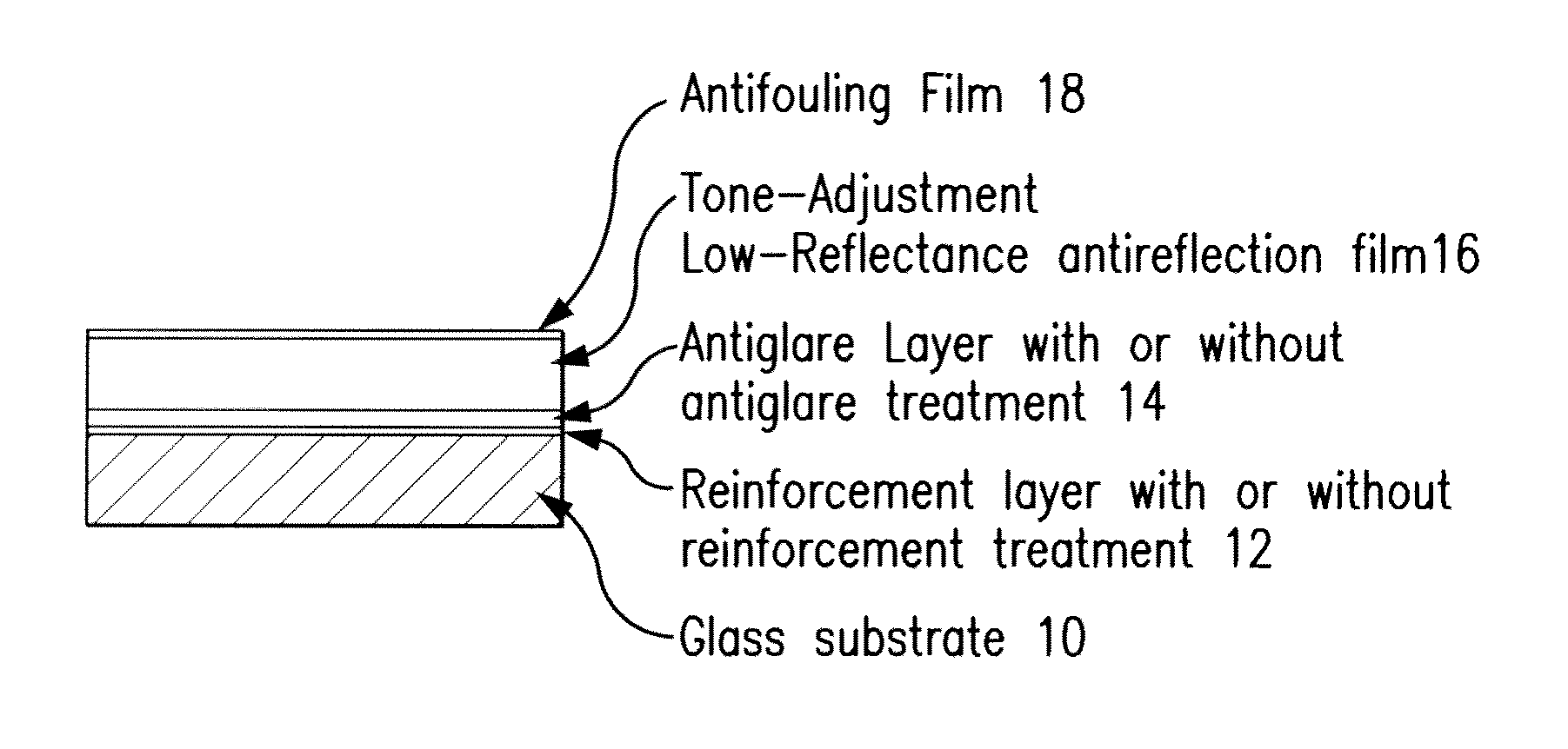
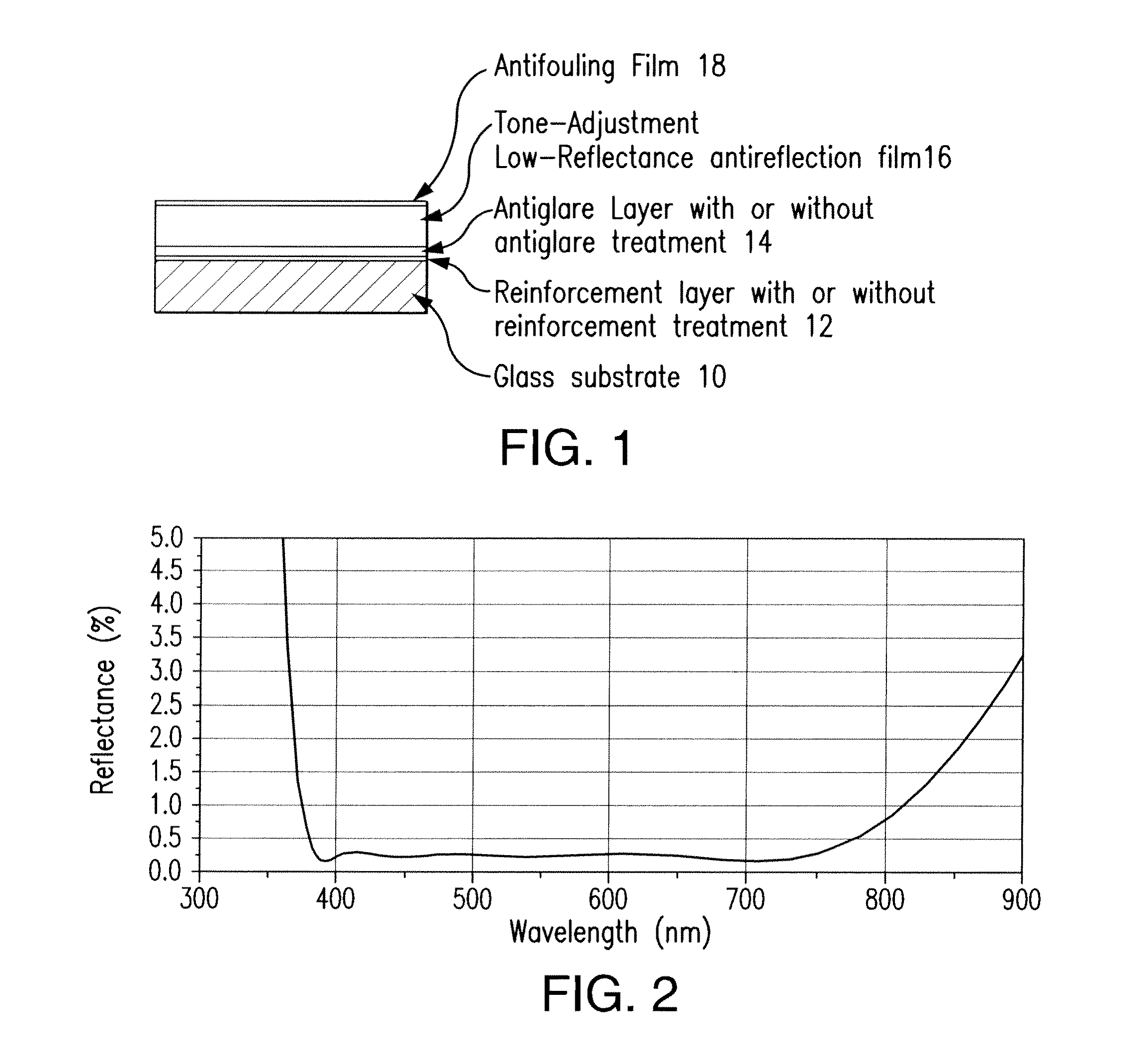
[0046]As an optical substrate 10, for example, a glass substrate exhibiting a refractive index of 1.52 was employed.
[0047]An antireflection film 16 having nine layers as specified in Table 1 was fabricated. Reinforcement treatment intended to prevent cracking was performed on the glass substrate 10, whereby a reinforcement layer was formed.
[0048]When the number of layers was equal to or smaller than eight, a wavelength band to be covered by the antireflection film 16 was narrowed. Accordingly, a change in a reflected color dependent on an incident angle of incident light that comes from outside was increased. However, when the number of layers was nine, the change in a reflected color dependent on the incident angle was limited, and cohesion between film materials was upgraded. When the antireflection film in the example 1 was employed in portable telecommunications equipment such as a smartphone, a display section of the equipment became easy to see because it was unsusceptible to ...
example 2
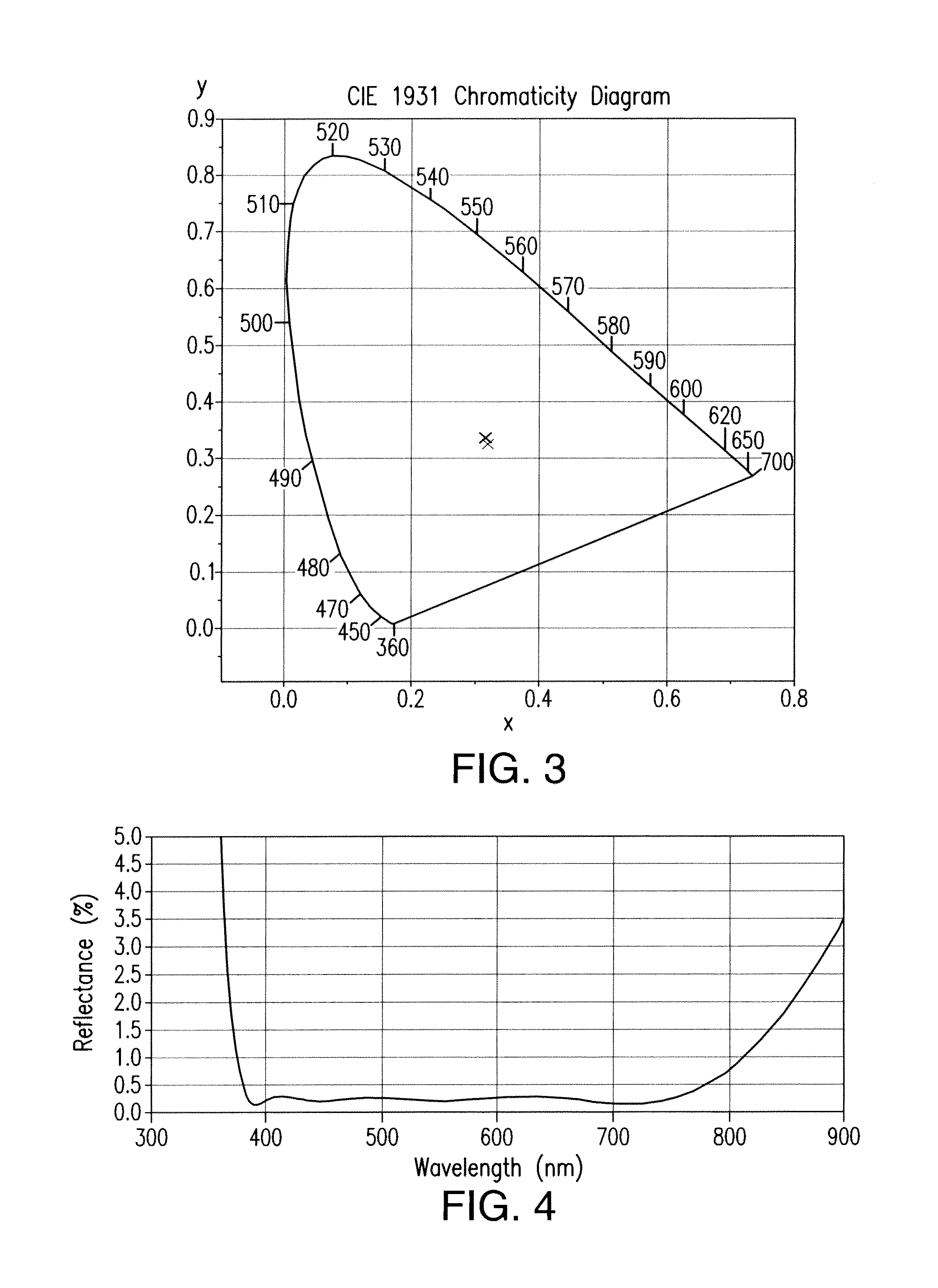
[0059]A substrate whose surface was subjected to antiglare treatment was adopted as a glass substrate 10. Incidentally, reinforcement treatment intended to prevent cracking was performed on the glass substrate 10, whereby a reinforcement layer was formed.
[0060]An antireflection film 16 having nine layers specified in Table 2 was fabricated.
[0061]When the number of layers was equal to or smaller than eight, a wavelength band to be covered by the antireflection film was narrowed. Accordingly, a change in a reflected color dependent on an incident angle of incident light that comes from outside was increased. However, when the number of layers was nine, the change in a reflected color dependent on the incident angle was limited, and cohesion between film materials was upgraded. When the antireflection film of the example 2 was employed in portable telecommunications equipment such as a smartphone, a display section became easy to see because it was unsusceptible to outside light and ha...
example 3
[0072]A substrate exhibiting a refractive index of 1.52 was adopted as a glass substrate 10.
[0073]The surface of the glass substrate 10 of the present example underwent neither antiglare treatment nor reinforcement treatment intended to prevent cracking.
[0074]An antireflection film 16 having ten layers specified in Table 3 was fabricated.
[0075]When the number of layers is equal to or smaller than eight, a wavelength band to be covered by the antireflection film was narrowed. A change in a reflected color dependent on an incident angle of incident light that comes from outside was increased. However, when the number of layers is ten, the change in a reflected color dependent on the incident angle was limited, and cohesion between film materials was upgraded. When the antireflection film of the example 3 was employed in portable telecommunications equipment such as a smartphone, a display section became easy to see because it was unsusceptible to outside light and hardly glared.
[0076]...
PUM
| Property | Measurement | Unit |
|---|---|---|
| wavelengths | aaaaa | aaaaa |
| wavelength | aaaaa | aaaaa |
| spectral reflectance | aaaaa | aaaaa |
Abstract
Description
Claims
Application Information
 - R&D
- Intellectual Property
- Life Sciences
- Materials
- Tech Scout
- Unparalleled Data Quality
- Higher Quality Content
- 60% Fewer Hallucinations
Browse by: Latest US Patents, China's latest patents, Technical Efficacy Thesaurus, Application Domain, Technology Topic, Popular Technical Reports.
© 2025 PatSnap. All rights reserved.Legal|Privacy policy|Modern Slavery Act Transparency Statement|Sitemap|About US| Contact US: help@patsnap.com