
Microelectromechanical three-axis capacitive accelerometer

a capacitive accelerometer, microelectromechanical technology, applied in acceleration measurement, measurement devices, instruments, etc., can solve the problem that none of these has proven optimized from the standpoint of dimensions, and achieve the effect of reducing dimensions and desired electrical characteristics

Active Publication Date: 2014-10-21
STMICROELECTRONICS SRL
View PDF19 Cites 8 Cited by
  • Summary
  • Abstract
  • Description
  • Claims
  • Application Information

AI Technical Summary

Benefits of technology

The present disclosure is about a MEMS accelerometer sensor that can be made smaller and have better electrical properties.

Problems solved by technology

Even though numerous types of MEMS three-axes accelerometers, with a wide range of geometrical configurations of the corresponding micromechanical structure have in fact been proposed, none of these has proven optimized from the standpoint of their dimensions.

Method used


Image

  • Microelectromechanical three-axis capacitive accelerometer
  • Microelectromechanical three-axis capacitive accelerometer
  • Microelectromechanical three-axis capacitive accelerometer

Examples


Embodiment Construction

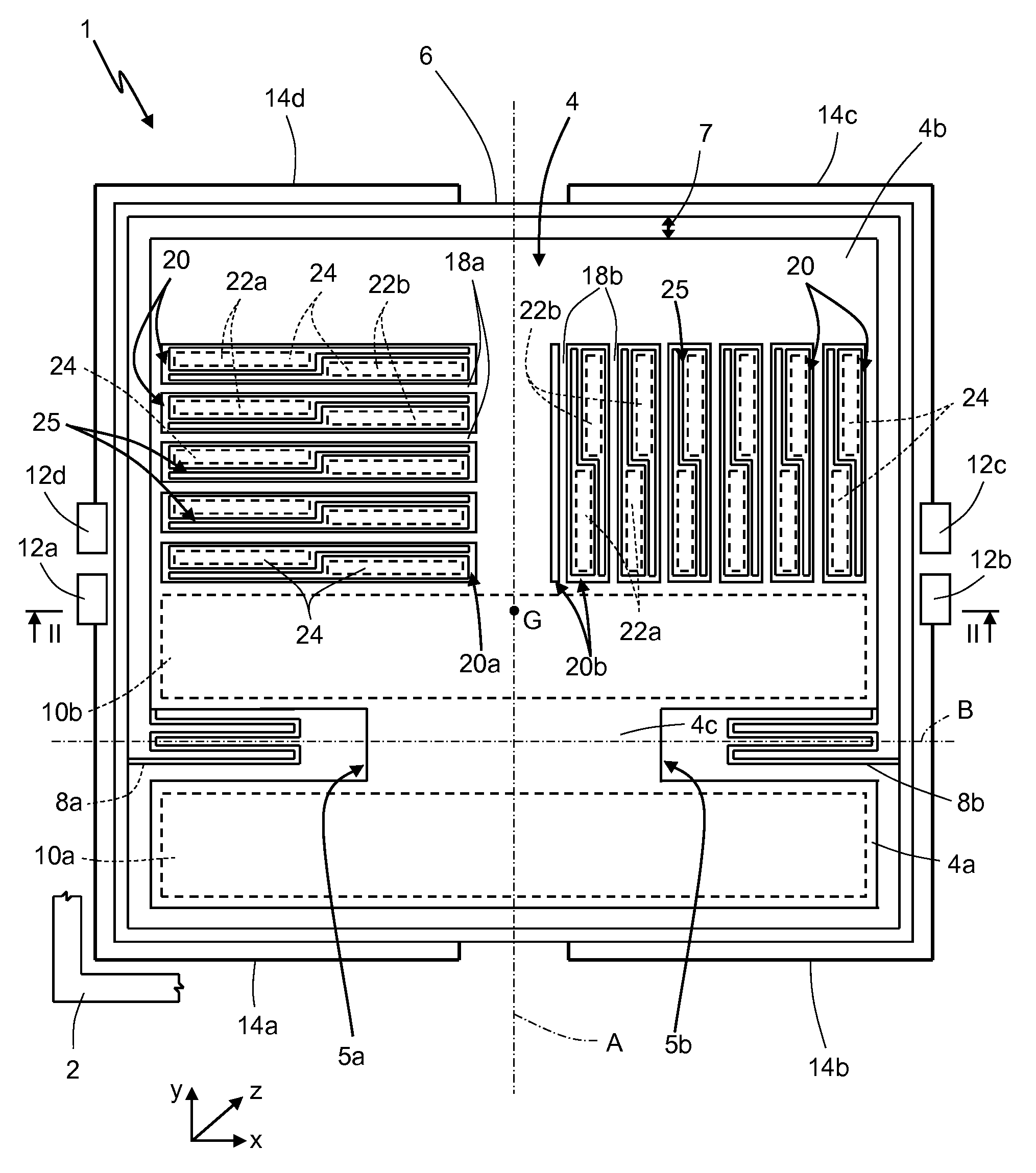
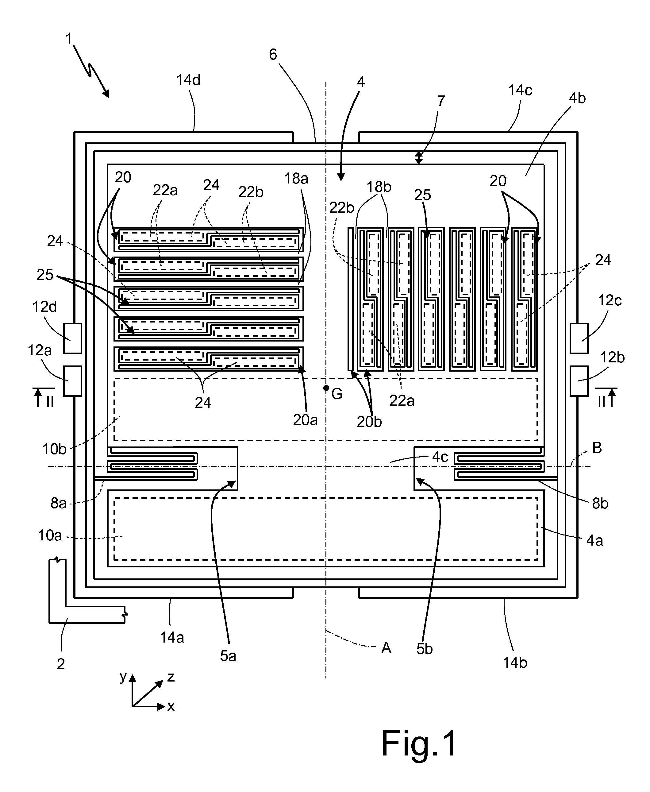
[0021]As will be discussed in detail in what follows, one aspect of the present disclosure envisages providing a MEMS three-axis accelerometer, of a capacitive type, comprising a single inertial mass, designed to enable detection of three mutually orthogonal components of acceleration, each directed along a corresponding detection axis of a set of three orthogonal axes, fixed with respect to a substrate, or to a package, of the same MEMS three-axis accelerometer. The single inertial mass is appropriately suspended above the substrate so that it is able to perform movements of detection along the three detection axes of the set of three orthogonal axes.

[0022]FIG. 1 shows a micromechanical structure 1, which is integrated in a die 2 of semiconductor material and is made with surface-micromachining processes, such as, for example, the THELMA (Thick Epi-poly Layer for Microactuators and Accelerometers) process (see for example: D. Galayko, A. Kaiser, B. Legrand, L. Buchaillot, C. Combi,...


PUM


Abstract

A micromechanical structure for a MEMS structure is provided with: a substrate; a single inertial mass having a main extension in a plane and arranged suspended above the substrate; and a frame element, elastically coupled to the inertial mass by coupling elastic elements and to anchorages, which are fixed with respect to the substrate by anchorage elastic elements. The coupling elastic elements and the anchorage elastic elements are configured so as to enable a first inertial movement of the inertial mass in response to a first external acceleration acting in a direction lying in the plane and also a second inertial movement of the inertial mass in response to a second external acceleration acting in a direction transverse to the plane.

Description

BACKGROUND[0001]1. Technical Field[0002]The present disclosure relates to a MEMS (Micro-Electro-Mechanical System) three-axis capacitive accelerometer.[0003]2. Description of the Related Art[0004]As is known, surface-micromachining techniques enable creation of MEMS structures within layers of semiconductor material, which have been deposited (for example, a layer of polycrystalline silicon) or grown (for example, a layer of epitaxial silicon) on top of sacrificial layers, which are removed via chemical etching.[0005]MEMS sensors made with the semiconductor technology are today used in a wide range of technological sectors, thanks to the small dimensions, versatility, and contained costs. In particular, accelerometer sensors are today widely used in the automotive field, for example in airbag systems, in stability-control systems (ESP®—Electronic Stability Program) and in brake-assist systems (ABS—Antilock Brake System), or in the field of consumer electronic devices, for example in...

Claims


Application Information

Patent Timeline
Patent Type & Authority Patents(United States)
IPC IPC(8): G01P15/18G01P15/125
CPCG01P15/125G01P15/18
Inventor FRANGI, ATTILIODE MASI, BIAGIOSIMONI, BARBARA
Owner STMICROELECTRONICS SRL
Learn More