Spatio-temporal directional light modulator
a directional light modulator and spatial-temporal technology, applied in optics, instruments, electrical equipment, etc., can solve the problems of reducing the brightness of the achievable display, occupying a portion of the image frame time, and increasing the total volume of the display, so as to reduce the power efficiency of the display system
- Summary
- Abstract
- Description
- Claims
- Application Information
AI Technical Summary
Benefits of technology
Problems solved by technology
Method used
Image
Examples
embodiment 600
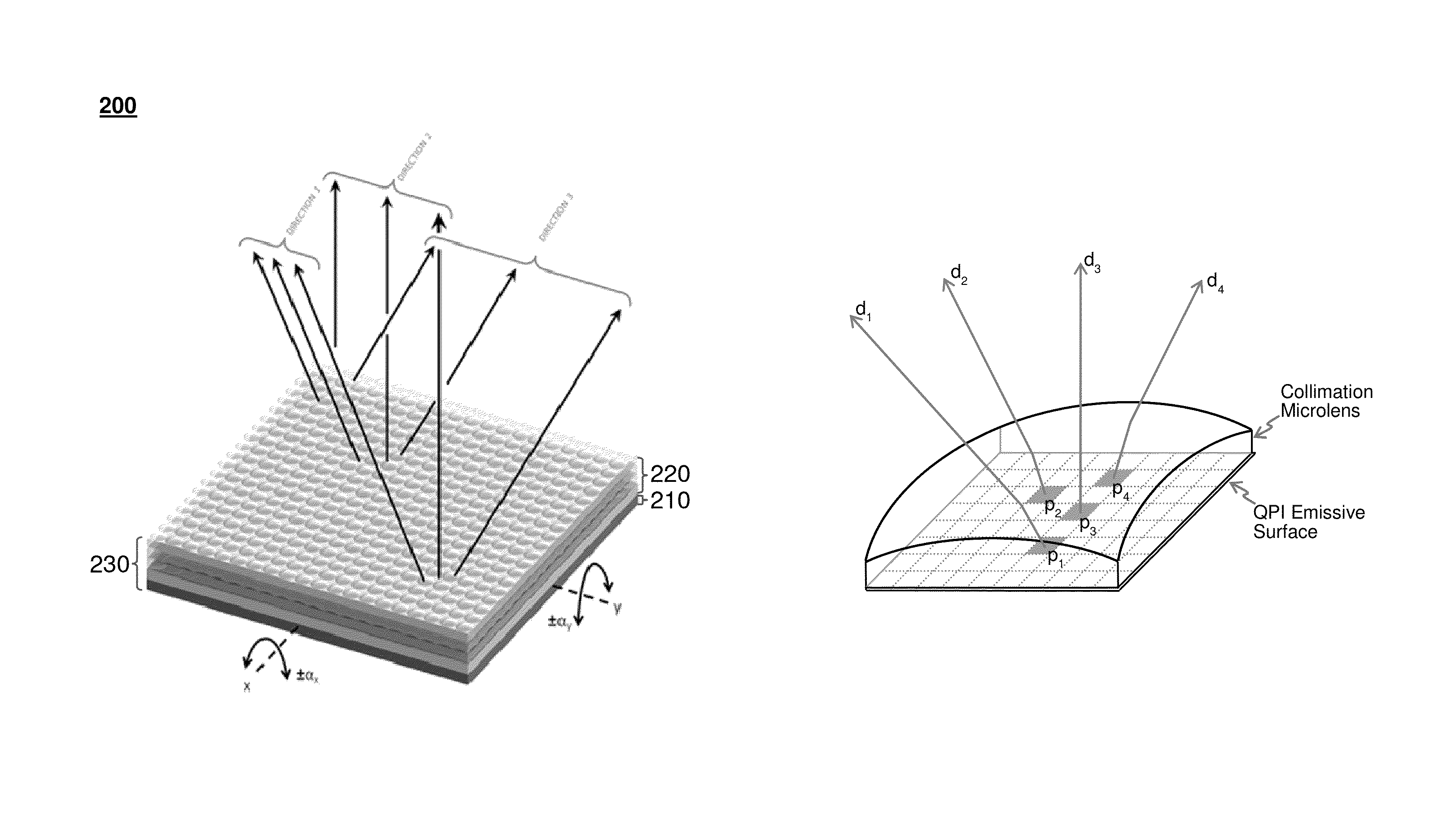
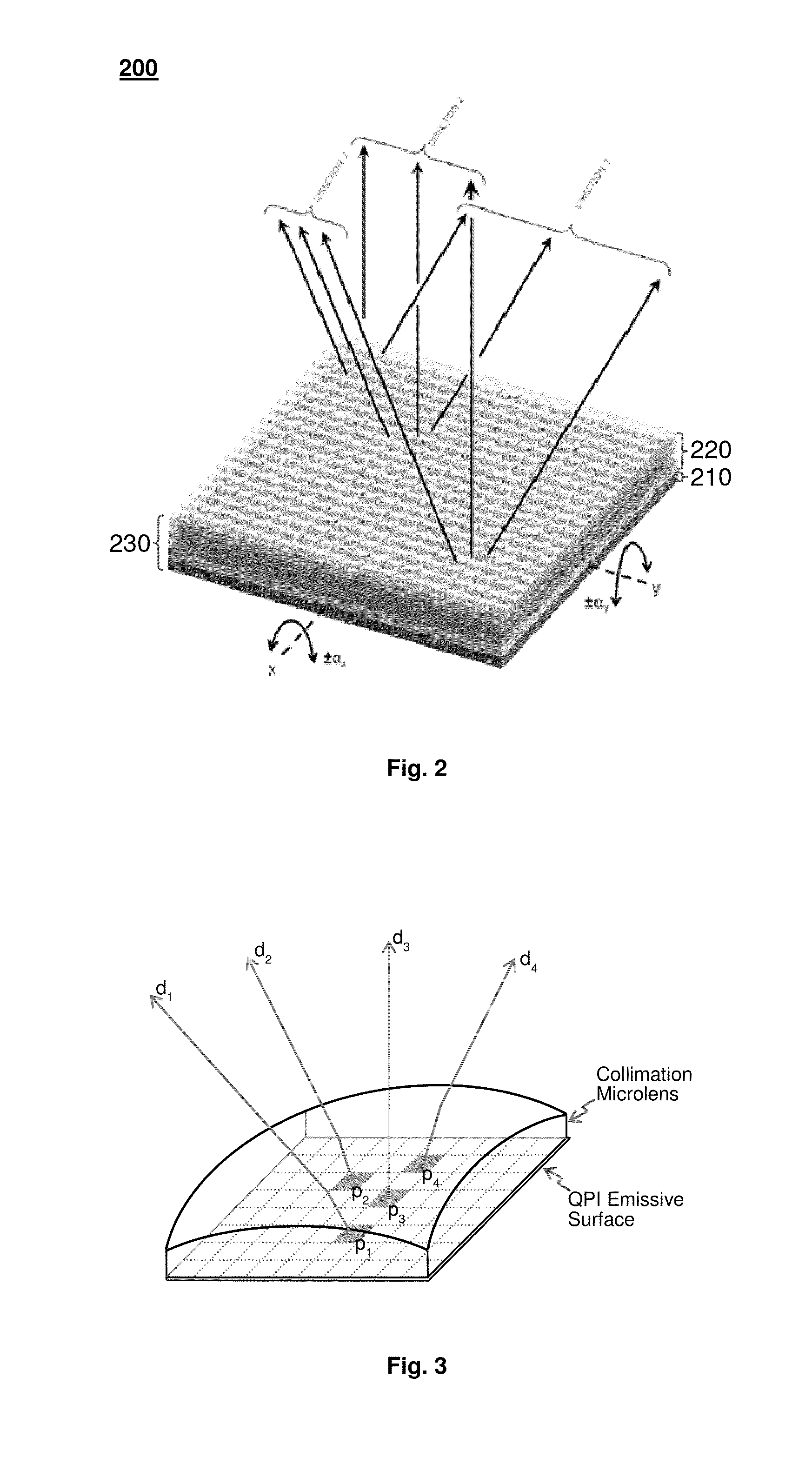
[0049]Referring to the side view illustration of FIG. 6, the articulation of the hinged interior segment 625 together with the bonded QPI / MLA assembly 230 would be accomplished using a set of electromagnets 635 placed at the four corners of the backside of the hinged interior segment 625, and a set of permanent magnets 636 placed on the topside of base layer 630 in alignment with the four corners of the backside of the hinged interior segment 625. The electromagnets 635 would be a coil having a metal core formed at wafer level using multilayer imprint lithography on the backside of the hinged interior segment 625. The permanent magnets 636 would be a thin magnetic strip typically of neodymium magnet (Nd2Fe14B) or the like. Articulation of the hinged interior segment 625 together with the bonded QPI / MLA assembly 230 as described earlier would be accomplished by driving the set of electromagnets 635 with an electrical signal having the appropriate temporal amplitude variation to affec...
embodiment 700
[0052]The hinged pad 721 / 735 is retained in place within the surface curvature of the pedestal 730 / 736 by the spring layer 725 which contains at each of its four corners a single spiral shaped spring 726 that is etched into the spring layer 725. As illustrated in FIG. 7 exploded view isometric, the inner end of each of the four spiral shaped springs incorporates an inner bonding pad 727 which corresponds to an identical bonding pad 722 located at the backside of the pad layer 721. Embedded within the spiral shaped springs 726 are multiple metal rails that are used to route the electrical interface signals from its inner bonding pad 727 to a set of contact pads 728 located at the peripheral edge of the backside of the spring layer 725. The edge contacts 728 on the backside of the outer end of the spring layer 725 correspond to a matching set of bonding pads 729 that are located at the peripheral edge of the base layer 730. The edge contacts on the topside of the base layer 730 are co...
PUM
| Property | Measurement | Unit |
|---|---|---|
| surface area | aaaaa | aaaaa |
| size | aaaaa | aaaaa |
| diameter | aaaaa | aaaaa |
Abstract
Description
Claims
Application Information
 - R&D
- Intellectual Property
- Life Sciences
- Materials
- Tech Scout
- Unparalleled Data Quality
- Higher Quality Content
- 60% Fewer Hallucinations
Browse by: Latest US Patents, China's latest patents, Technical Efficacy Thesaurus, Application Domain, Technology Topic, Popular Technical Reports.
© 2025 PatSnap. All rights reserved.Legal|Privacy policy|Modern Slavery Act Transparency Statement|Sitemap|About US| Contact US: help@patsnap.com


