Table for use in plasma processing system and plasma processing system
a plasma processing system and plasma technology, applied in chemical/physical/physical-chemical processes, coatings, chemical/physical/physical-chemical processes, etc., can solve the problems of poor within-wafer uniformity of etched wafers, poor field strength of plasma etched wafers, and inability to obtain. , to achieve the effect of improving the uniformity of within-substrates, reducing field strength, and high field strength
Active Publication Date: 2014-06-03
TOKYO ELECTRON LTD
View PDF12 Cites 9 Cited by
- Summary
- Abstract
- Description
- Claims
- Application Information
AI Technical Summary
Benefits of technology
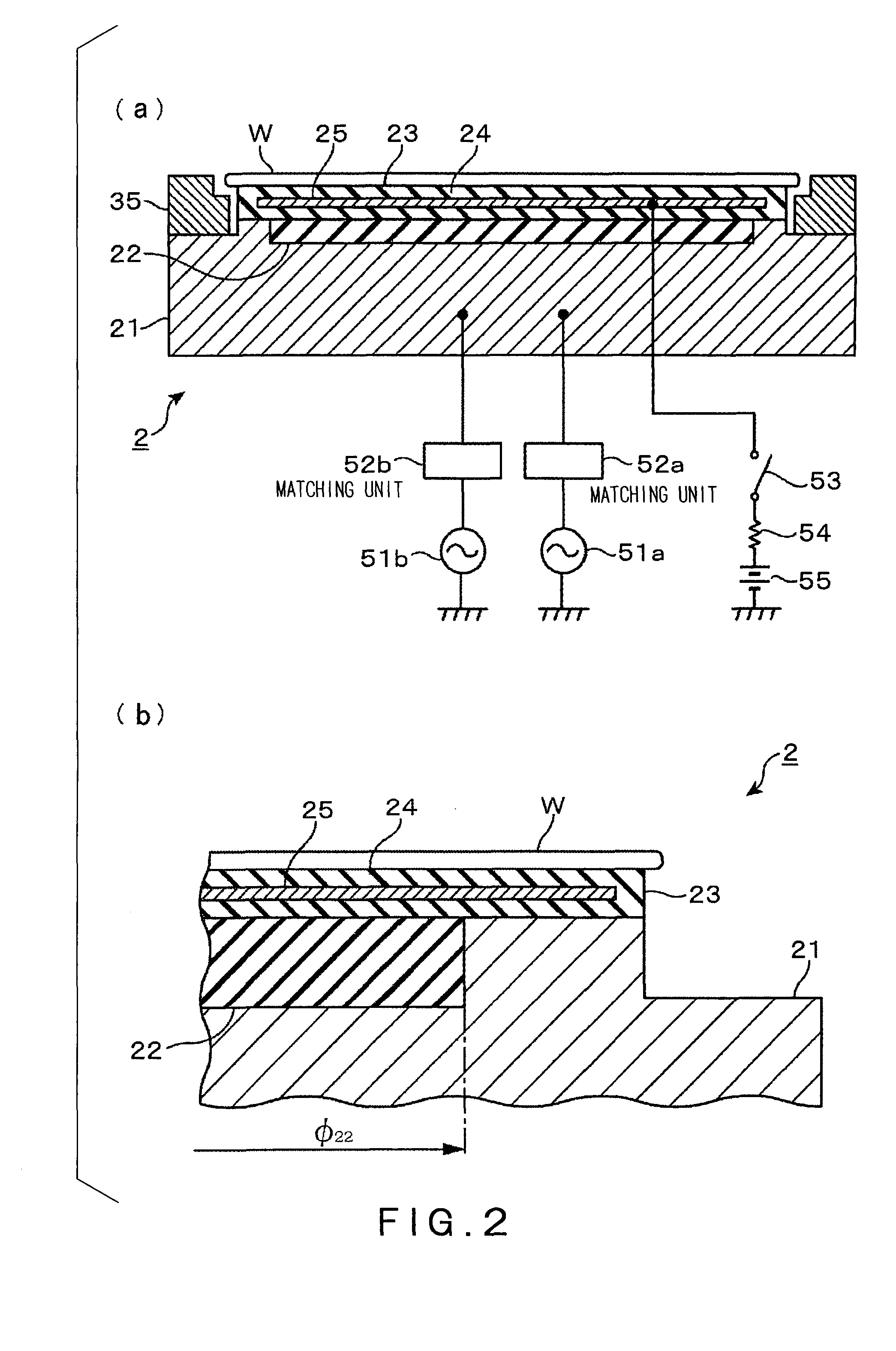
The present invention provides a table for a plasma processing system that can increase the rate of processing the edge of a substrate with plasma and improve the uniformity of processing across the substrate. The table has an electrically conductive member connected to an RF generator for plasma formation and a first dielectric layer to create a high-frequency electric field uniform across the substrate. A second dielectric layer with a high relative dielectric constant is embedded in the center of the table to prevent high-frequency current from leaking and allow it to cause cavity cylindrical resonance of TM mode more efficiently. This results in a more uniform electric field in the substrate plane and improved processing results.
Problems solved by technology
Method used
View moreImage
Smart ImageViewing Examples
Examples
example 1
[0058]The relative dielectric constant ∈24 of the upper dielectric layer 24 was set to 100.
example 2
[0059]The relative dielectric constant ∈24 of the upper dielectric layer 24 was set to 900.
Login to View More PUM
| Property | Measurement | Unit |
|---|---|---|
| relative dielectric constant | aaaaa | aaaaa |
| frequency | aaaaa | aaaaa |
| dielectric constant | aaaaa | aaaaa |
Abstract
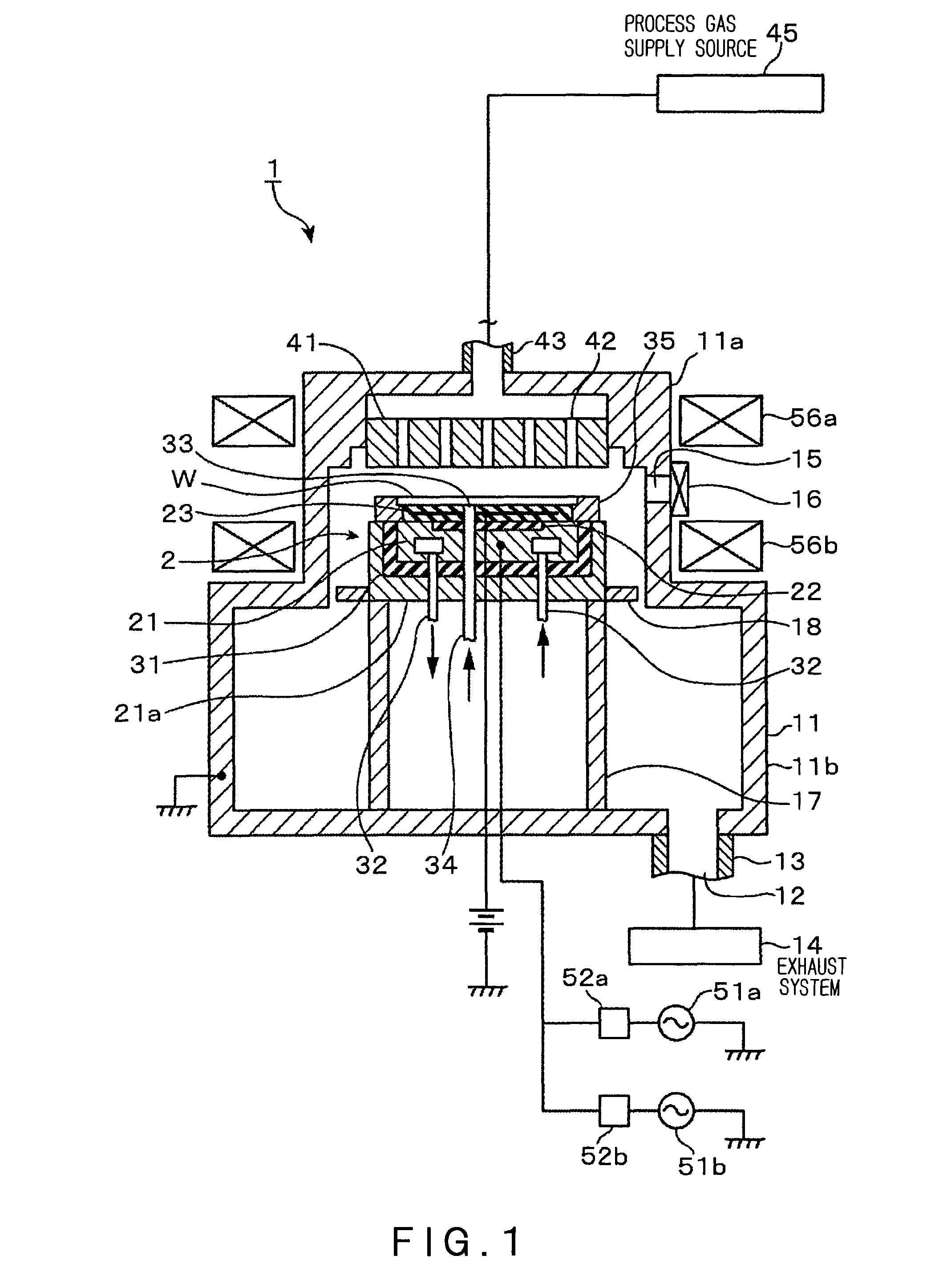
Disclosed herein is a table 2 for use in a plasma processing system 1 that includes an electrically conductive member serving as a lower electrode 21 for plasma formation, a lower dielectric layer 22 (first dielectric layer) formed on the electrically conductive member so that it covers the center of the upper surface of the electrically conductive member, serving to make a high-frequency electric field to be applied to plasma via a substrate uniform, and an upper dielectric layer 24 (second dielectric layer) having a relative dielectric constant of 100 or more, formed on the electrically conductive member so that it is in contact at least with the edge of the substrate, in order to prevent a high-frequency current that has propagated along the electrically conductive member face from leaking to the outside of the substrate (wafer W).
Description
CROSS REFERENCE TO PRIOR APPLICATIONS[0001]This application claims priority from U.S. Provisional Application No. 60 / 844,368 filed on Sep. 14, 2006, and Japanese Patent Application No. 2006-217873 filed on Aug. 10, 2006. The entire contents of these applications are incorporated herein by reference.BACKGROUND OF THE INVENTION[0002]1. Field of the Invention[0003]The present invention relates to a table on which a substrate to be subjected to plasma processing, such as a semiconductor wafer, is placed, and to a plasma processing system comprising the table.[0004]2. Background Art[0005]The process of semiconductor device production includes many processing steps in which a process gas is made into plasma and this plasma is used to process a substrate, such as dry etching and ashing. Of the plasma processing systems in which plasmas are used to process substrates, a processing system of the following type is often used: a pair of parallel plate electrodes are placed in a processing syst...
Claims
Login to View More Application Information
Patent Timeline
 Patent Type & Authority Patents(United States)
IPC IPC(8): H01L21/306C23F1/00C23C16/50C23C16/00
CPCH01J37/32532H01J37/32082H01J37/32009
Inventor KOSHIISHI, AKIRAHIMORI, SHINJIMATSUYAMA, SHOICHIRO
Owner TOKYO ELECTRON LTD
Features
- R&D
- Intellectual Property
- Life Sciences
- Materials
- Tech Scout
- Unparalleled Data Quality
- Higher Quality Content
- 60% Fewer Hallucinations
Learn More Browse by: Latest US Patents, China's latest patents, Technical Efficacy Thesaurus, Application Domain, Technology Topic, Popular Technical Reports.
© 2025 PatSnap. All rights reserved.Legal|Privacy policy|Modern Slavery Act Transparency Statement|Sitemap|About US| Contact US: help@patsnap.com


