
Systems for single pass parallel hierarchical timing closure of integrated circuit designs

a technology of integrated circuit design and hierarchical timing, which is applied in the direction of cad circuit design, program control, instruments, etc., can solve the problems of complex and time-consuming task of designing these integrated circuits, complicating the evaluation of the overall circuit design, and increasing the complexity of integrated circuit design

Active Publication Date: 2013-09-17
CADENCE DESIGN SYST INC
View PDF34 Cites 13 Cited by
  • Summary
  • Abstract
  • Description
  • Claims
  • Application Information

AI Technical Summary

Benefits of technology

The invention provides a new way to analyze the timing of functions in a computer chip. It takes into account the time it takes for clock signals to travel through different parts of the chip, so that different parts can be timed independently. This helps improve the overall timing of the chip. The invention also allows for better timing of data signals in the chip.

Problems solved by technology

Integrated circuits have become larger and more complex to provide additional functionality and / or improved performance.
The task of designing these integrated circuits is also very complex and time consuming, involving synthesizing, analyzing and optimizing many circuit parameters.
However, dividing up an integrated circuit design into multiple blocks and hierarchical levels can complicate the evaluation of the overall circuit design.
However, dividing the semiconductor chip hierarchically and implementing it through software is a complex and involved process.
Timing budgets for data paths are usually automatically generated in early design stages when the integrated circuit design may be incomplete or have errors so that generated timing budgets may require manual correction and analysis.
However, the load on a clock path within a partition may by significant such that the clock path also requires time budgeting across partitions.

Method used


Image

  • Systems for single pass parallel hierarchical timing closure of integrated circuit designs
  • Systems for single pass parallel hierarchical timing closure of integrated circuit designs
  • Systems for single pass parallel hierarchical timing closure of integrated circuit designs

Examples


Embodiment Construction

[0024]In the following detailed description of the embodiments of the invention, numerous specific details are set forth in order to provide a thorough understanding of the present invention. However, it will be obvious to one skilled in the art that the embodiments of the invention may be practiced without these specific details. In other instances well known methods, procedures, components, and circuits have not been described in detail so as not to unnecessarily obscure aspects of the embodiments of the invention.

Introduction

[0025]The embodiments of the invention facilitate budgeting of clock signal timing between functional blocks or modules of an integrated circuit design as part of the time budgeting flow or methodology. Time budgeting divides the time for a data signal to propagate along the data path across block boundaries. In this case, time budgeting also divides the time for the clock signal (clock division) to propagate along the clock paths across block boundaries. Tha...


PUM


Abstract

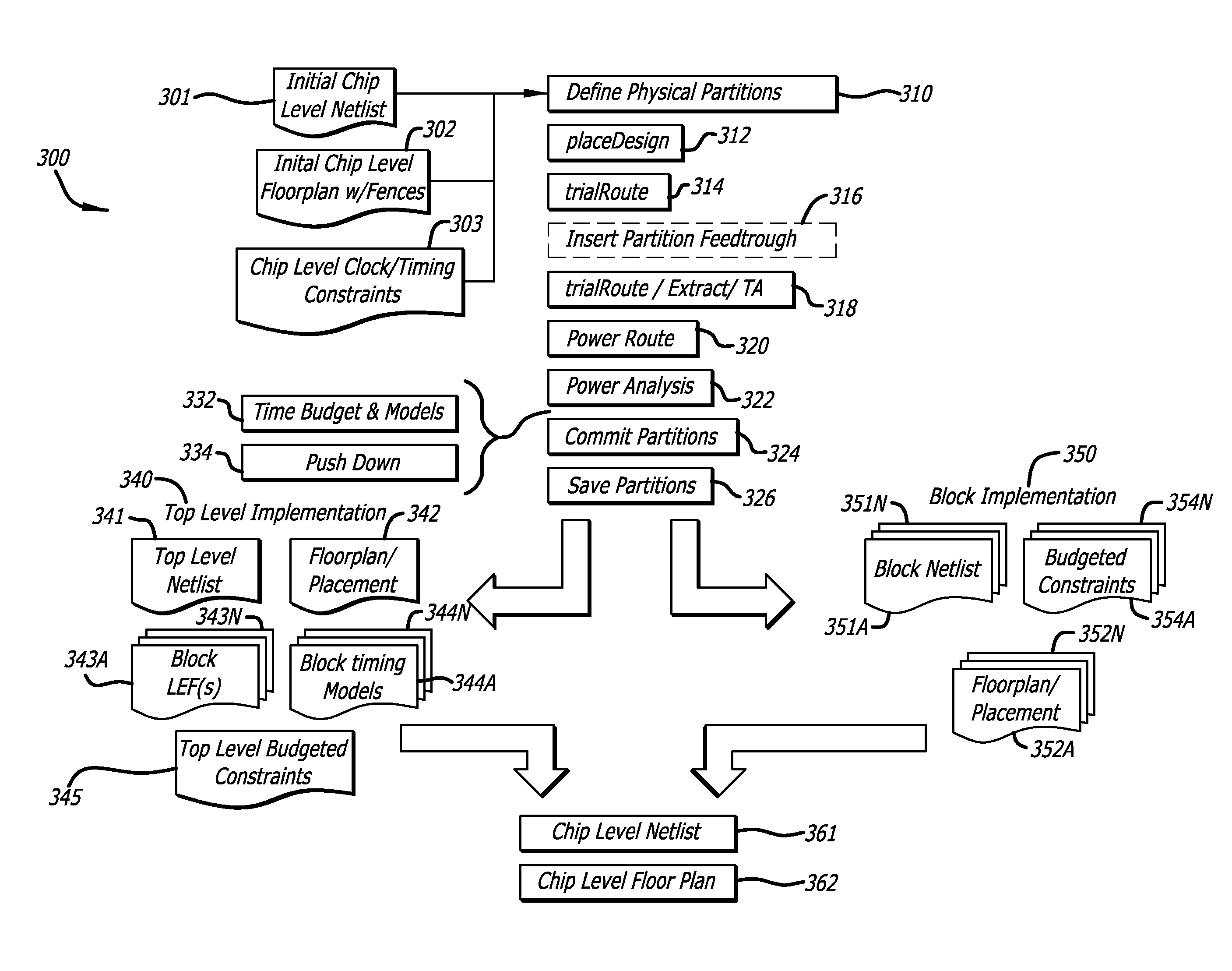
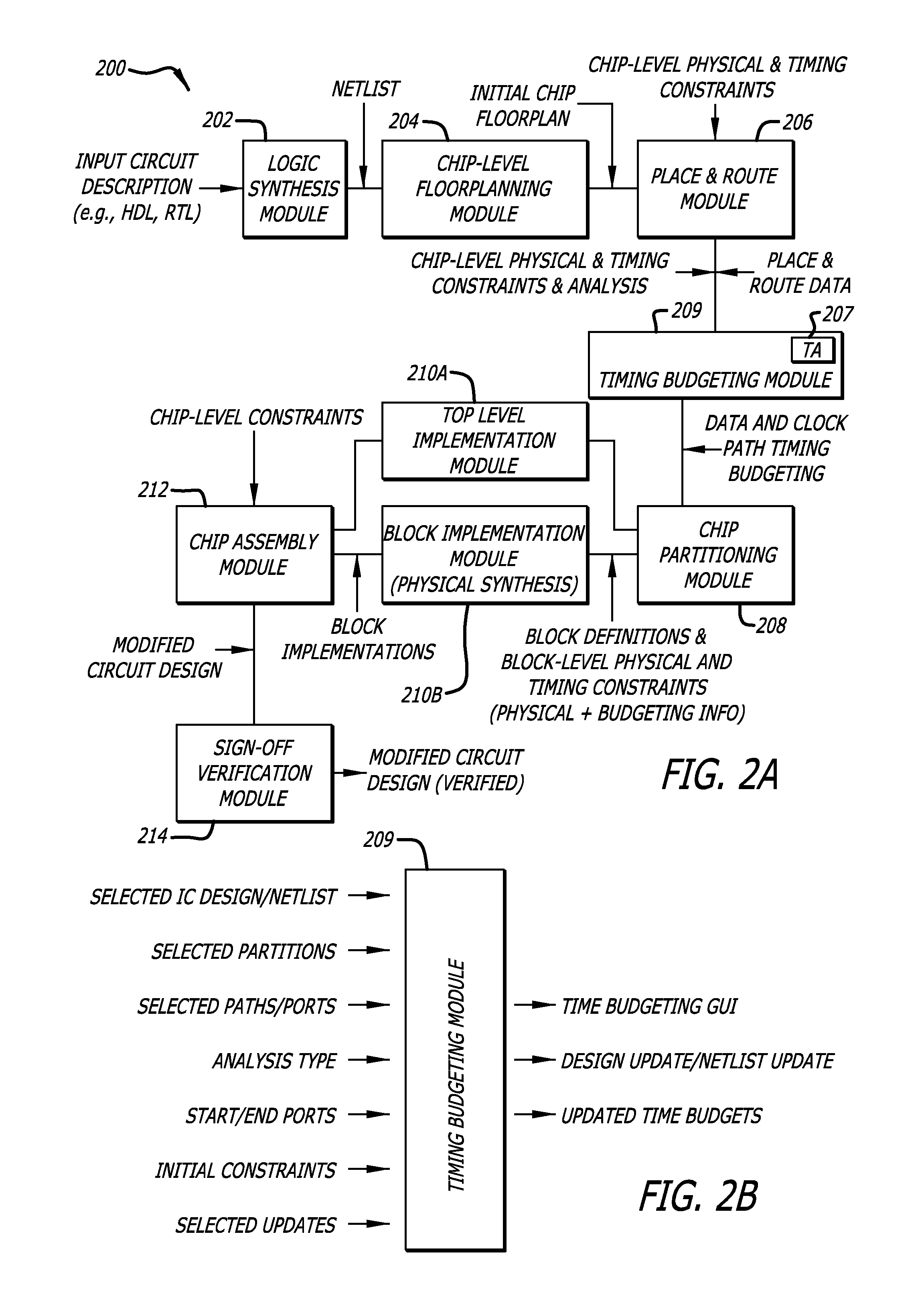
In one embodiment of the invention, a method includes partitioning an integrated circuit design into a hierarchy of a top level and a plurality of partitions, wherein the top level includes a top level netlist and each partition includes a partition netlist; receiving data path timing budgets and clock path timing budgets for each of the plurality of partitions of the integrated circuit design; and generating a timing budget model of each partition in response to the respective data path timing budgets and clock path timing budgets, wherein each timing budget model includes an intra-partition clock timing constraint for each respective partition for independent implementation of the top level.

Description

CROSS-REFERENCE TO RELATED APPLICATIONS[0001]This non-provisional United States (U.S.) patent application is a divisional and claims the benefit of U.S. patent application Ser. No. 12 / 708,530 filed on Feb. 18, 2010 by inventors Vivek Bhardwaj, et al., entitled FLOW METHODOLOGY FOR SINGLE PASS PARALLEL HIERARCHICAL TIMING CLOSURE OF INTEGRATED CIRCUIT DESIGNS, now allowed. U.S. patent application Ser. No. 12 / 708,530 claims the benefit of U.S. Provisional Patent Application No. 61 / 265,705 entitled FLOW METHODOLOGY FOR SINGLE PASS PARALLEL HIERARCHICAL TIMING CLOSURE OF INTEGRATED CIRCUIT DESIGNS filed on Dec. 1, 2009 by inventors Vivek Bhardwaj et al.; and is a continuation in part and claims the benefit of pending U.S. patent application Ser. No. 12 / 437,096 entitled USER INTERFACE FOR TIMING BUDGET ANALYSIS OF INTEGRATE CIRCUIT DESIGNS filed on May 7, 2009 by inventors Vivek Bhardwaj et al., incorporated by reference. U.S. patent application Ser. No. 12 / 708,530 is also continuation i...

Claims


Application Information

Patent Timeline
Patent Type & Authority Patents(United States)
IPC IPC(8): G06F17/50
CPCG06F17/505G06F17/5068G06F2217/84G06F30/327G06F2119/12G06F30/30G06F30/39G06F30/396G06F30/3312
Inventor BHARDWAJ, VIVEKLEVITSKY, OLEGGUPTA, DINESH
Owner CADENCE DESIGN SYST INC
Learn More