
Non-volatile variable resistance memory device and method of fabricating the same

a variable resistance and memory device technology, applied in the direction of bulk negative resistance effect devices, semiconductor devices, electrical equipment, etc., can solve the problems of loss of all stored data, low integration density, and relatively low operating speed compared to drams, and achieve variable resistance characteristics and stable reset currents.

Active Publication Date: 2013-09-03
SAMSUNG ELECTRONICS CO LTD
View PDF54 Cites 3 Cited by
  • Summary
  • Abstract
  • Description
  • Claims
  • Application Information

AI Technical Summary

Benefits of technology

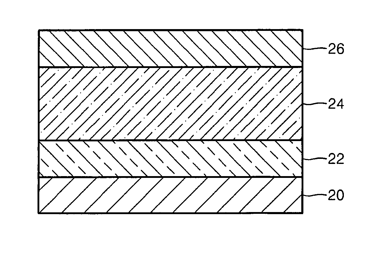
The buffer layer stabilizes reset currents and maintains reliable switching characteristics over repeated cycles, reducing reset current levels and enhancing the memory device's integration density and operational stability.

Problems solved by technology

The DRAM may have advantages of relatively high integration density and relatively high operating speed, but when the power supply is shut down, it may lose all its stored data.
Unlike a volatile memory, the flash memory may have characteristics of non-volatility, but it may have a relatively low integration density and a relatively low operating speed compared to those of the DRAM.
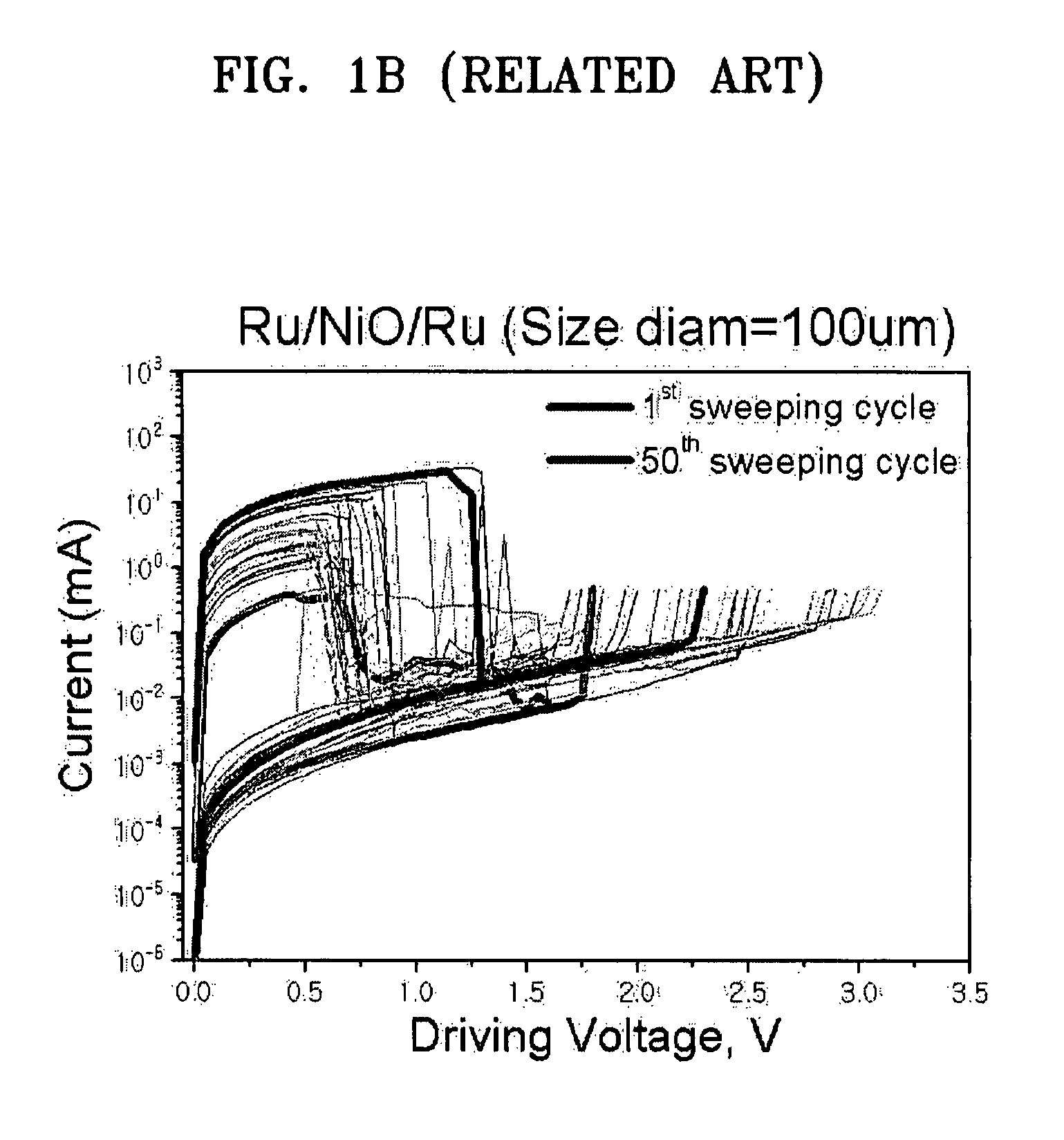
Operation voltage may be increased and reset voltage may be increased, which causes the reliability of the memory device to decrease.

Method used


Image

  • Non-volatile variable resistance memory device and method of fabricating the same
  • Non-volatile variable resistance memory device and method of fabricating the same
  • Non-volatile variable resistance memory device and method of fabricating the same

Examples


Embodiment Construction

[0025]Hereinafter, a variable resistance memory device according to example embodiments will be explained in detail with reference to the accompanying drawings. In the drawings, the thicknesses of layers and regions are exaggerated for clarity.

[0026]Spatially relative terms, such as “beneath,”“below,”“lower,”“above,”“upper” and the like, may be used herein for ease of description to describe one element or feature's relationship to another element(s) or feature(s) as illustrated in the figures. It will be understood that the spatially relative terms are intended to encompass different orientations of the device in use or operation in addition to the orientation depicted in the figures. For example, if the device in the figures is turned over, elements described as “below” or “beneath” other elements or features would then be oriented “above” the other elements or features. Thus, the example term “below” may encompass both an orientation of above and below. The device may be otherwis...


PUM


Abstract

A non-volatile variable resistance memory device and a method of fabricating the same are provided. The non-volatile variable resistance memory device may include a lower electrode, a buffer layer on the lower electrode, an oxide layer on the buffer layer and an upper electrode on the oxide layer. The buffer layer may be composed of an oxide and the oxide layer may have variable resistance characteristics.

Description

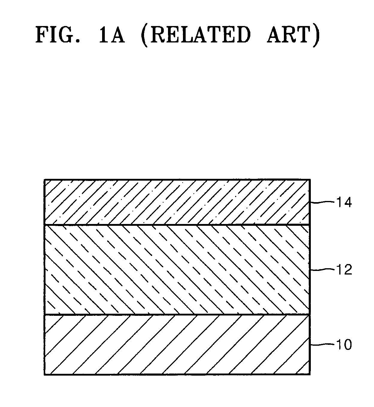
PRIORITY STATEMENT[0001]This application claims priority under 35 U.S.C. §119 to Korean Patent Application No. 10-2006-0040389, filed on May 4, 2006, in the Korean Intellectual Property Office (KIPO), the entire contents of which are incorporated herein by reference.BACKGROUND[0002]1. Field[0003]Example embodiments relate to a non-volatile variable resistance memory device and a method of fabricating the same. Other example embodiments relate to a non-volatile variable resistance memory device employing a buffer layer on a lower electrode of the memory device including a transition metal oxide having variable resistance characteristics, thereby to result in a decrease of a reset current and a method of fabricating the same.[0004]2. Description of the Related Art[0005]Much effort has been made to develop semiconductor devices that have an increased number of memory cells per unit area, for example, an increased integration density and may be operated at relatively high speed and with...

Claims


Application Information

Patent Timeline
Patent Type & Authority Patents(United States)
IPC IPC(8): H01L29/02
CPCH01L45/12H01L45/146H01L45/1233H01L45/04H10N70/801H10N70/20H10N70/8833H10N70/826H10B99/00
Inventor BOURIM, EL MOSTAFALEE, EUN-HONGCHO, CHOONG-RAE
Owner SAMSUNG ELECTRONICS CO LTD
Learn More